Leave A Message
If you are interested in our products and want to know more details,please leave a message here,we will reply you as soon as we can.
submit

Blog

Home

Blog

  • SFP Cage Dimensions and PCB Footprint: What Engineers Need to Know
    SFP Cage Dimensions and PCB Footprint: What Engineers Need to Know
    Sep 07, 2026
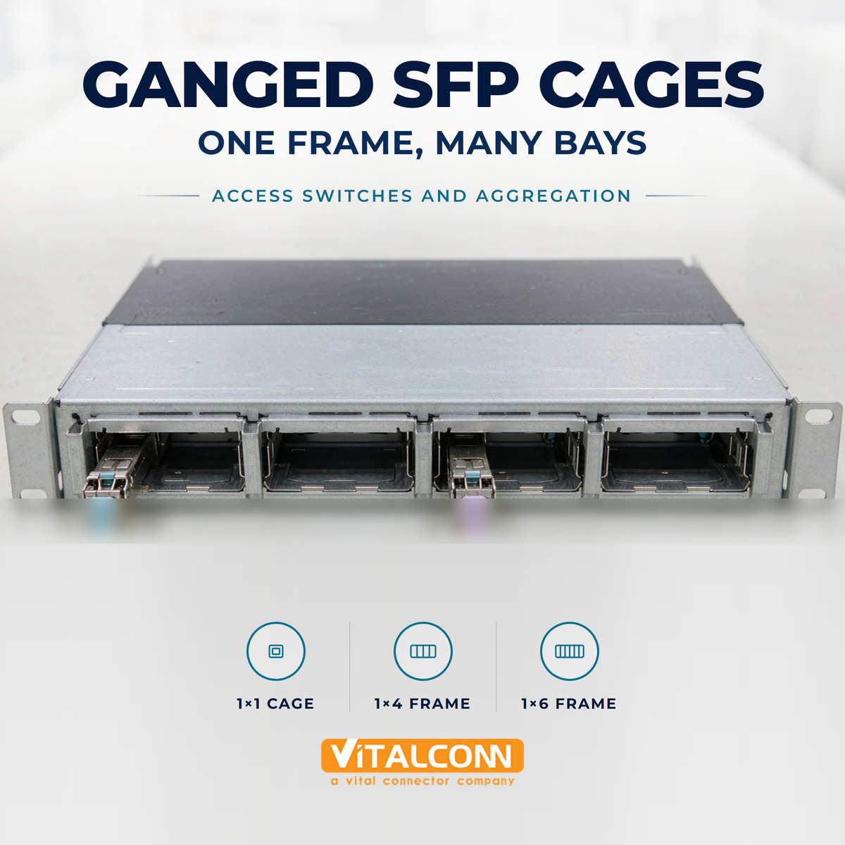
    SFP Cage Dimensions: Start From the Module, Not the Connector Every SFP cage dimensions question begins with the pluggable module that will live inside it. SFP and SFP+ modules follow the multi-source agreement (MSA) drawings — SFF-8074/SFF-8432 for the module body — so the cage's inside profile, module insertion depth, and connector engagement zone are fixed by the MSA, not by the cage vendor. What vendors differ in is everything around that fixed core: cage length, EMI features, heatsink options, port count, and the SFP cage footprint that lands on your PCB. This is why two cages that accept the same modules can have completely different board consequences. The section below breaks down the dimension variables that actually change your layout, then covers the footprint and keep-out rules that decide whether the first prototype board assembles cleanly. The Dimension Variables That Matter to Your Board Cage length is the first variable. The module body itself occupies a fixed depth; the cage must fully contain that depth plus the bezel feature that presents the port at the front panel. Longer cages add depth above the board — which matters in 1U enclosures where the lid clearance is measured in millimeters. Extended-length cages move the module's hot end further from the board, sometimes helping airflow, but consuming enclosure depth. Dimension Variable What It Changes Design Impact Cage overall length Enclosure depth, module support 1U chassis clearance, front-panel protrusion Port count (1×1, 1×2, 1×4…) Facepanel width occupied Port pitch must match panel standard Connector vs cage offset Where the 20-pin connector sits Footprint position relative to panel line Heatsink provision Crown surface, side walls Thermal path for the module EMI features Finger count, gasket type Bezel cutout tolerance class Mounting leg geometry SMT / press-fit / TH pattern Pad pattern and anchor placement Port pitch deserves special attention for ganged cages. A 1×4 cage presents four module slots at a fixed center-to-center spacing; that spacing must match your facepanel cutout pattern and your routing escape plan. Because the high-speed differential pairs from each connector must reach their PHY or switch die with matched lengths, the ganged part's fixed pitch propagates directly into your length-matching budget. SFP Cage Footprint: Reading the Vendor Drawing Correctly The SFP cage footprint is more than a pad pattern. A complete footprint package includes the 20-pin connector contact pad layout, the mounting leg pads, the mechanical keep-out where no components may sit (the cage body overhangs the board), and the bezel cutout drawing for the front panel. The most common first-spin error we see is treating the mechanical keep-out as advisory — the cage's sheet-metal skirt extends over the board beyond the pads, and any component placed in that shadow will collide at assembly. Verify the connector pad layout against the specific SFP (SFF-8432) or SFP+ (SFF-8431) contact assignment — do not assume a drawing from a different part family transfers. Respect the full mechanical keep-out including the cage skirt and any EMI finger features that dip toward the board. Check the recommended panel cutout and its tolerance class; EMI gaskets and spring fingers only seal when the cutout is within the specified band. For press-fit cages, confirm hole diameters, plating, and annular rings against the drawing before releasing the PCB fab data. SFP Cage PCB Layout Rules for Signal and Power Good SFP cage PCB layout practice keeps the high-speed pairs short and symmetric. The 20-pin interface carries differential pairs for TX and RX, plus single-ended control signals (TX_FAULT, TX_DISABLE, RX_LOS, MOD_ABS, rate select) and power (3.3 V). Route the differential pairs as coupled 100 Ω lines with minimal via count, keep them away from the cage wall to avoid shield-coupled crosstalk, and return every layer change with an adjacent ground via. Ground strategy connects the footprint to the EMI system. The connector's shield legs and the cage's mounting legs should tie to a solid ground region that is stitched to chassis at controlled points — not scattered vias that create circulating currents. The 3.3 V power feed wants local decoupling near the connector, sized for hot-plug inrush, because plugging a module is an uncontrolled power event on your rail. Thermal Envelope: Dimensions With a Temperature Attached Cage dimensions and thermal design are inseparable. The module dissipates its heat into the cage structure — mainly through the crown spring fingers that press against the module's top surface — and the heat then crosses the cage's mounting interface into the board and the panel. When you compare cage dimensions, compare them at equal thermal intent: a bare cage and a cage with an integrated or clip-on heatsink have different depth and height envelopes but also different module temperature outcomes. Our companion articles cover this in depth: the SFP cage heatsink guide for heatsink selection, and the thermal management article for airflow-first designs. For the electrical shielding side of the same mechanical features, see SFP cage EMI shielding. Verification Checklist Before Releasing the Board Cross-check the cage outline in your PCB CAD against the vendor's 2D drawing in both plan and elevation views. Confirm the front-panel cutout, its tolerance, and the gap to adjacent RJ45 or SFP ports on the same panel. Walk the mechanical keep-out component by component — connectors, LEDs, test points, and fiducials are the usual victims. Review the escape routing of the first differential pair on the endmost port of a ganged cage; if it cannot escape, no port can. Re-run the thermal estimate with the chosen cage's heat path, at worst-case module power, in the real enclosure airflow. For mixed RJ45/SFP panels, do the combined floorplan — our guides on RJ45 port configurations and on SFP cage vs SFP+ differences cover the adjacent constraints. Cage Height and Bezel Options: SFP Cage Dimensions Nobody Specs Early The length and width of an SFP cage come from the module, but the height and the bezel are chosen by the designer, and they are the two dimensions most often changed after the first mechanical mock-up. Cages are available in standard nose heights and low-profile heights; the low-profile variants save vertical space but reduce the volume available for EMI gaskets and for the spring fingers that wipe the module. If the product has a tight 1U chassis, verify that the low-profile cage still accepts the tallest module on the qualified list, not just the one shipped with the evaluation kit. The bezel is the face of the cage at the panel: single-port, duplex (two ports in one stamped frame), or ganged multi-port frames that span 4, 8, or 12 ports. Duplex and ganged frames hold tighter port-to-port pitch than individually soldered cages, which matters when the front panel is laser-cut to a fixed pattern. They also carry fewer separate grounding paths to the panel, which simplifies the EMI bonding strategy. The cost is that a bent corner on a ganged frame affects multiple ports, so handling instructions for the assembly line should be written accordingly. Top-entry versus bottom-entry cages change which side of the board the module slides in from, and therefore which side needs clearance above the connector footprint Nose height must clear the panel thickness plus any gasket compression, typically 0.5 to 1.0 mm Duplex and ganged frames improve pitch accuracy; single cages are easier to rework one port at a time Pull tabs and bail latches on modules need clearance behind the panel opening, not just in front of it One practical check we run before freezing the mechanical drawing: slide the longest qualified module into the cage on the actual board, inside the actual chassis, and connect a cable with the latch closed. Module bodies vary by a few millimeters between vendors, and a drawing that fits the shortest module can still block a cable bend radius. Discovering this at the mock-up stage costs an afternoon; discovering it at the certification lab costs a schedule. Frequently Asked Questions (FAQ) Are SFP cage dimensions standardized? The internal profile that accepts the module is standardized by the SFP MSA specifications (SFF-8074/SFF-8432, SFF-8431 for SFP+), but cage outer dimensions, length, EMI features, and heatsink options vary by manufacturer and part family. What is the difference between cage dimensions and the PCB footprint? Cage dimensions describe the mechanical envelope of the connector assembly, while the PCB footprint defines the pads, keep-out zones, and panel cutout that the part requires on the board. Both come from the vendor drawing and must be used together. What is the keep-out area on an SFP cage footprint? The keep-out is the board region covered by the cage body and its mounting features where no components may be placed. Placing parts in this shadow is one of the most common first-spin errors in SFP board design. Do ganged 1xN cages change port pitch requirements? Yes. Ganged cages fix the center-to-center spacing of adjacent ports, which must match your front-panel standard and your routing escape plan for the high-speed differential pairs. How does cage length affect thermal performance? Longer cages can move the module's hottest region further from heat-sensitive board components and sometimes improve airflow, but they consume enclosure depth. The thermal benefit depends more on crown spring contact and heatsink design than on length alone. Need the Right SFP Cage Connector for Your Application? Get samples, full datasheets, and FAE support from VITALCONN's SFP cage connector product line. Explore SFP Cage Connectors Request Samples
    Read More
  • RJ45 Connector Types Explained: 1×1, 1×N and 2×N Port Configurations
    RJ45 Connector Types Explained: 1×1, 1×N and 2×N Port Configurations
    Sep 04, 2026
    When engineers talk about RJ45 connector types, they usually mean the port configuration first: 1×1, 1×N, or 2×N. A 1x1 RJ45 connector is a single, independent jack. A 1×N part gangs N jacks side by side in one housing — 1×2, 1×4, 1×6, 1×8 — sharing a shield frame and LED position pattern. A 2×N part stacks two of those rows vertically, so a 2×4 gives you eight ports in the depth of one row. The configuration choice drives PCB panel area, port pitch, airflow, LED routing, and even which switch ASIC you can support. This guide walks through each family, the trade-offs between ganged and stacked housings, and the selection points our application team raises most often with networking customers. Configuration Ports Typical Product Key Characteristic 1×1 1 Routers, gateways, IPC Independent housing, free placement 1×2 / 1×4 2–4 Small switches, firewalls Shared frame, consistent pitch 1×6 / 1×8 6–8 Workgroup switches Single-row density for front panels 2×2 4 NICs, compact appliances Two rows, half the width 2×4 / 2×6 8–12 Enterprise line cards Maximum faceplate density The 1×1 RJ45 Connector: Maximum Placement Freedom The single-port jack is the smallest building block and the most flexible. Each 1×1 connector can be placed wherever the board needs it, rotated to face any panel edge, and sourced independently of any other port. In products with one to four Ethernet ports — industrial gateways, security cameras, home routers — designers almost always pick discrete 1×1 jacks because the port count is too low to benefit from ganging. A 1×1 part also isolates mechanical stress. A user inserting a cable with force on port three of a ganged assembly flexes the whole housing; with discrete jacks the stress stays local. And on mixed-density products where port spacing is set by other connectors (SFP cages, USB, console ports), discrete jacks adapt to irregular pitch that no ganged part matches. For the underlying pinout shared by every one of these jacks, see our RJ45 pinout diagram and wiring guide. 1×N Ganged RJ45 Connectors: The Switch Workhorse Ganged single-row connectors exist for one reason: dense, uniform port fields. When a switch faceplate needs eight identical RJ45 ports in a row, a 1×8 connector guarantees the port pitch is uniform, the LED positions align with the silkscreen, and the shield frame is one continuous EMI structure instead of eight separate ones. Assembly benefits too: one placement instead of eight, and one shield interconnect instead of many. The trade-offs are structural. A long ganged housing concentrates insertion force across the whole part, so the mounting legs and their anchor pads must be specified with the full-width assembly in mind — coplanarity tolerance over the length of the housing is the number SMT engineers watch. Individual port replacement is impossible; a damaged port means replacing the whole part. And the fixed pitch of the ganged family must match your facepanel standard, which is usually set by the industry-common port pitch for the switch class you are building. Ganged parts share one shield frame — verify the shield ground path is continuous across every port segment. LED options (single, dual-color, or none) are fixed per part family; pick them before panel graphics are frozen. Long housings need support at both ends and at intermediate legs to control solder-joint stress. Stacked RJ45 Connector (2×N): Doubling Faceplate Density A stacked RJ45 connector puts a second row of jacks directly above the first, doubling port count at the same faceplate width. A 2×4 replaces two 1×4 parts with one component and half the panel length; on line cards and NICs where every millimeter of facepanel is revenue, this is the deciding factor. Stacking changes three engineering conversations. Mechanically, the part is tall, so retention under cable pull and vibration depends on mounting legs at both rows plus the shared housing body. Thermally, two rows of magnetics in one body concentrate heat — for 2×N magnetic jacks, check the temperature-rise data at full PoE load on every port simultaneously, not per port. In layout, routing the upper row's signals under and past the lower row constrains the escape channels, so early floorplanning with the connector's footprint drawing is essential. Orientation and Entry Options Across RJ45 Connector Types Independent of port count, RJ45 jacks come in right-angle (side entry, tab up or tab down) and vertical (top entry) orientations. Right-angle with the latch tab down is the common switch faceplate arrangement; tab-up variants exist for compact products where the cable exits upward. Vertical jacks save depth and are used where boards plug into a backplane or where the cable exits the top of an enclosure. Orientation Best For Watch Out For Right-angle, tab down Standard switch/router faceplate Latch interferes with panels below Right-angle, tab up Dense 2×N stacking, compact cases Less common; verify availability Vertical (top entry) Backplane modules, depth-limited cases Cable management above the board Magnetic Versus Non-Magnetic Within Each Configuration Every port configuration above exists in both magnetic and non-magnetic variants, and the configuration choice interacts with that one. A 2×N magnetic jack concentrates up to sixteen transformers in one body, so its thermal and crosstalk specifications carry more weight than a 1×1 part's. A 1×N non-magnetic part paired with a discrete magnetics array spreads the heat but consumes routing area exactly where density was the goal. Our magnetic RJ45 vs non-magnetic RJ45 comparison covers the electrical side in detail. Selection Checklist for Port Configuration Start from the facepanel standard: total ports, port pitch, and the height available for one or two rows. Compare total board cost, not connector cost: ganged parts cut placements but add coplanarity and stress risk. For 2×N magnetic jacks, demand full-port simultaneous thermal data, especially for PoE designs. Confirm LED style, light-pipe geometry, and legend alignment before the housing is frozen. Check the footprint drawing against your routing channels — especially upper-row escape in stacked parts. For products with mixed RJ45 and SFP ports, floorplan both connector families together; see our SFP cage guides for the adjacent constraints. If you are evaluating connectors for a full design rather than a single port question, our RJ45 connector buying guide and the Ultimate Guide to RJ45 connectors cover shield styles, plating, and manufacturer evaluation criteria. LED Indicators and Panel Details Across RJ45 Connector Types Port configuration is the headline decision, but two details ride along with it and cause just as many late-stage changes: LED indication and the panel interface. Most RJ45 connector types are offered with integrated dual-color LEDs (green for link, amber for activity), discrete LED pockets beside each port, or no LED provision at all. Ganged 1×N and stacked 2×N parts with integrated LEDs simplify assembly dramatically, because the operator no longer has to align eight separate light pipes with the front panel cutouts. The trade-off is serviceability: if one LED channel fails on a ganged part, the entire connector is replaced. When discrete LEDs are used, check the light-pipe alignment tolerance against the front-panel cutout early. We have seen projects where the panel drawing allowed ±0.4 mm on cutout position while the PCB-to-panel stack-up already consumed ±0.3 mm in standoff and hole tolerances, leaving almost nothing for connector placement accuracy. Stacked RJ45 connector parts make this worse, because the upper row of light pipes sits that much farther from the board and amplifies any tilt in the assembly. Integrated dual-color LEDs: fastest assembly, standard on most ganged parts; verify current-limiting resistors are on the board, not expected inside the jack Discrete LEDs with light pipes: flexible, but demand a tolerance stack review between PCB, connector, and panel No LEDs: common on industrial ports where status is reported through management software instead Panel bezels: many stacked and ganged parts accept an optional front bezel that hides mounting screws and improves EMI contact with the panel Panel mounting itself deserves a decision, not a default. Ear tabs and integrated studs anchor the connector to the panel so insertion forces never reach the solder joints. This matters most in high port-count panels where a technician plugging stiff Category 6A cables applies real side load. Our recommendation for any panel with more than four ports is simple: choose an RJ45 connector type with panel retention features, and let the PCB carry signals rather than mechanical load. Frequently Asked Questions (FAQ) What does 1xN mean in RJ45 connectors? 1×N describes a ganged connector with one row of N RJ45 ports in a shared housing — for example 1×4 for four ports in a row. It contrasts with 1×1 (a single independent jack) and 2×N (two stacked rows). What is a stacked RJ45 connector? A stacked RJ45 connector (2×N) places a second row of jacks directly above the first, doubling port count at the same faceplate width. A 2×4 part provides eight ports in the width normally used by four. When should I use individual 1x1 jacks instead of a ganged connector? Use 1×1 jacks when port count is low (typically under four), when ports must sit at irregular spacing, or when independent mechanical stress isolation and per-port serviceability matter more than placement efficiency. Do ganged RJ45 connectors improve EMI performance? A ganged connector provides one continuous shield frame across all ports, which simplifies shield grounding compared to several separate jacks. Performance still depends on the shield design and grounding of the specific part family.Can 2xN stacked connectors support PoE on all ports at once? Yes, when the part is specified for it. Because the magnetics of both rows share one housing, verify the datasheet's thermal-rise data for all ports powered simultaneously rather than extrapolating single-port ratings. Need Help Choosing the Right Connector? VITALCONN Electronics manufactures a full range of RJ45, SFP, USB-C, SIM, and SD card connectors with integrated magnetics, EMI shielding, and PoE support. Contact our application engineers for specifications, samples, and cross-reference support. View RJ45 Connector Request Samples
    Read More
  • SIM Card Socket Types: Nano SIM vs Micro SIM vs Standard SIM
    SIM Card Socket Types: Nano SIM vs Micro SIM vs Standard SIM
    Sep 02, 2026
    Choosing a SIM card socket starts with one question: which SIM form factor does your device accept? The three card sizes — standard (mini), micro, and nano — share the same electrical interface but differ completely in mechanical envelope, and the socket must match the card exactly. A board designed for a Nano SIM socket saves more than half the footprint of the old standard-SIM part, which is why nano has become the default in routers, IoT modules, POS terminals, and automotive telematics. This guide covers the three form factors, the contact assignments behind every SIM interface, the insertion mechanisms (push-push versus push-pull versus hinged), and the practical selection factors — detection switch, insertion cycles, ESD, and shielding — that separate a socket that lasts from one that fails in the field. Form Factor Card Dimensions Thickness Introduced Where Used Today Standard SIM (2FF, mini) 25.0 × 15.0 mm 0.76 mm 1996 Legacy industrial, M2M devices Micro SIM (3FF) 15.0 × 12.0 mm 0.76 mm 2010 Older IoT modules, tablets Nano SIM (4FF) 12.3 × 8.8 mm 0.67 mm 2012 Phones, routers, telematics, POS Standard SIM: The Legacy Format That Refuses to Die The standard SIM, also called 2FF or mini-SIM, is the full-size ID-1-derived card cut down to 25 × 15 mm. Its large body makes it mechanically forgiving: the socket contacts are bigger, the insertion guides are longer, and the card is easy to handle with gloves in industrial environments. Many long-lifecycle M2M and metering products still specify standard-SIM sockets because the format was locked in when the design was qualified, and changing it would trigger recertification. The cost of that compatibility is PCB area. A standard-SIM socket occupies roughly three times the board area of a nano part and stands taller, which constrains slim enclosures. For new designs there is rarely a reason to choose it unless the card supply chain or a legacy module dictates otherwise. Micro SIM Socket: The Middle Ground The Micro SIM socket accepts the 3FF card at 15 × 12 mm and offers a reasonable balance between contact robustness and footprint. It was the mainstream choice between roughly 2010 and 2015, and it remains common on industrial cellular modules where the module vendor's evaluation kit was built around micro SIM. Electrically it is identical to the other formats — same eight contacts, same protocol — so the choice is purely mechanical. Designers migrating a micro-SIM board to nano often use a socket that accepts the card through an adapter frame, but adapters add tolerance stack-up and are best limited to development, not production. If footprint pressure exists, move the layout to nano directly rather than carrying an adapter permanently. Nano SIM Socket: Today's Default Nano SIM at 12.3 × 8.8 mm and 0.67 mm thickness is the smallest of the three and the current standard for consumer and most industrial devices. A quality nano SIM socket compensates for the small card with precision molded guide rails, a stiff contact spring design, and a detect switch integrated into the frame. Because the card is thin and light, the retention mechanism — push-push latching or a hinged cover — does most of the mechanical work. At this scale, contact design quality matters more than in the larger formats. Look for gold-plated contacts (typically 0.1 µm minimum on the contact area), a specified normal force (usually 1–2 N per contact), and a rating of at least 10,000 insertion cycles for field-serviceable devices. Contact wipe length during insertion — how far the contact slides across the pad — is what self-cleans oxidation, and it is a real difference between socket families. Contact Assignments: The Same Eight Pads on Every Card Every SIM, regardless of size, presents the same contact layout defined by ISO/IEC 7816. The socket maps these pads to your board through either 6 or 8 contacts, and modern sockets almost always bring out all eight. Contact Signal Function C1 VCC Supply voltage (1.8 V / 3 V) C2 RST Reset from host C3 CLK Clock up to 5 MHz (class follow) C4 Reserved / USB Unused in classic SIM; USB in USB-IC cards C5 GND Ground reference C6 VPP Programming voltage (unused, often grounded) C7 I/O Bidirectional data line C8 Reserved / USB Unused in classic SIM; USB in USB-IC cards Hot-swap support deserves attention: when a card can be changed while the system runs, the socket's detect switch (a mechanical switch that closes when a card is fully seated) lets the host power down the interface cleanly before removal. Route the detect pin with a pull-up and debounce it in firmware; never let contact bounce trigger card-reset logic directly. Insertion Mechanisms: Push-Push, Push-Pull, and Hinged The insertion mechanism is independent of card size, and it drives both user experience and long-term reliability. Push-push sockets latch the card on insertion and eject it on a second push — the smartphone behavior — with a spring and slider mechanism inside. They protect the card and feel right in consumer products, but the mechanism adds height and cost, and a jammed slider in a dusty environment can lock the card. Push-pull sockets rely on contact friction to retain the card and offer lower height and cost, at the price of user discipline. Our detailed comparison in push-push vs push-pull card socket covers the reliability physics. Hinged types, where a cover flips open to receive the card, provide the best retention and are common in automotive telematics, where vibration is constant and the card must never walk out. For the broader card-connector family — SD, microSD, smart card — see the card socket connector guide. Selection Factors Beyond the Form Factor Factor What to Check Why It Matters Insertion cycles 5,000–10,000+ rating for serviceable devices Contact spring fatigue sets socket life Detection switch Presence, travel, debounce spec Hot-swap and firmware card-state logic ESD exposure Air-gap to user; TVS placement on I/O and VCC SIM pads are a touch point for users Shielding Metal shield over contacts if specified RF modules nearby radiate into card traces Mounting SMT coplanarity, anchor pads for retention Vibration pulls sockets off the board Operating temperature -40 °C to +85 °C for industrial/automotive Spring force drops with plastic creep Common Failure Modes and How Good Sockets Avoid Them Contact oxidation from insufficient wipe — choose sockets with longer contact travel. Detect switch failure from dust ingress — prefer sealed or shielded variants in dirty environments. Solder joint cracking under vibration — add anchor pads and use SMT legs with flexible geometry. Card ejection failure in push-push after shock — verify the slider mechanism's shock rating, not just static retention. Plastic fatigue at high temperature — check the housing resin rating (LCP or high-temp nylon) against your thermal profile. Whatever form factor and mechanism your design settles on, the socket is a mechanical wear part with an electrical job. Treating insertion cycles, wipe, and retention as first-class specifications — the way we specify them in our own SIM card connector series — is what keeps a connected product connected for its whole service life. Frequently Asked Questions (FAQ) What are the three SIM card sizes? Standard (mini) SIM is 25 × 15 mm, micro SIM is 15 × 12 mm, and nano SIM is 12.3 × 8.8 mm. All three use the same eight-contact electrical interface; only the mechanical envelope differs.Can a nano SIM socket accept a micro SIM card? No. The socket guide rails match one card size exactly. Adapters can physically let a nano card sit in a micro socket, but adapters add tolerance and are not recommended for production designs. What is the difference between push-push and push-pull SIM sockets?Push-push sockets latch the card and eject it with a second push using an internal slider. Push-pull sockets retain the card by contact friction only. Push-push protects the card better; push-pull is lower and cheaper. What does the detect switch on a SIM card socket do? The detect switch closes when a card is fully seated, letting the host detect insertion and removal. It enables safe hot-swap by powering the interface down before the contacts separate. How many insertion cycles should a SIM socket support? For field-serviceable devices, specify at least 10,000 cycles for user-accessible sockets. Internal M2M sockets that are inserted once at production can accept lower ratings, typically 1,000–5,000 cycles. Need Help Choosing the Right Connector? VITALCONN Electronics manufactures a full range of RJ45, SFP, USB-C, SIM, and SD card connectors with integrated magnetics, EMI shielding, and PoE support. Contact our application engineers for specifications, samples, and cross-reference support. View SIM Card Socket Cross-Reference Tool
    Read More
  • SFP Cage Mounting Types Compared: SMT vs Press-Fit vs Through-Hole
    SFP Cage Mounting Types Compared: SMT vs Press-Fit vs Through-Hole
    Aug 31, 2026
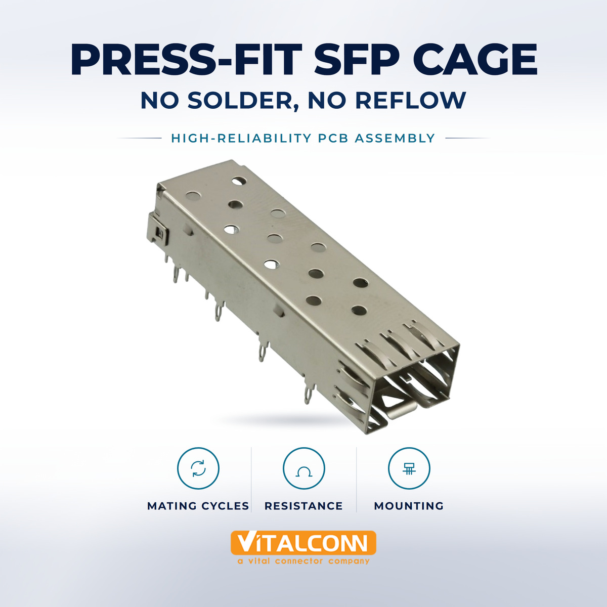
    SFP cage mounting is not a packaging detail — it defines how your optical module cage attaches to the PCB, how it survives thermal cycling, and how easy it is to rework. An SFP cage is a sheet-metal shield that surrounds the 20-contact SFP connector and guides the pluggable module into place. The cage and its connector are attached to the board through mounting legs or tabs, and those attachments come in three main styles: SMT (surface-mount technology), SFP press-fit, and through-hole solder. Each represents a different trade-off between assembly cost, mechanical strength, and long-term reliability. Because the cage carries the EMI shielding function and must hold alignment tolerances against a module that will be inserted and removed hundreds of times, the mounting interface is a structural element of the design. Choosing the wrong type shows up later as coplanarity failures at reflow, shield-ground intermittent contact, or cracked solder joints after thermal cycling in the field. Attribute SMT Mounting Press-Fit Mounting Through-Hole Solder Attachment Tabs soldered on board surface Compliant pins pressed into plated holes Legs inserted and wave/reflow soldered Assembly process Standard reflow with the connector Press operation, no solder, no heat Wave solder or pin-in-paste reflow Rework Moderate — hot air desolder Easy — press out, minimal board stress Difficult — through-hole desolder Mechanical strength Good with adequate tabs Excellent — mechanically interlocked Excellent Thermal cycling reliability Good Excellent — compliant pins flex with CTE mismatch Good Extra process step None Press operation after reflow Wave/paste step if not pin-in-paste Typical use Cost-sensitive commercial boards Telecom, industrial, high-reliability Legacy designs, heavy mechanical loads SFP Cage SMT Mounting: The Default for Modern Boards In SFP cage SMT construction, the cage legs and connector leads are formed as flat surface-mount tabs that go through the same reflow oven as the rest of the SMT assembly. The key advantage is process simplicity: the cage is just another reel-fed or tray-fed component, and no second assembly operation is needed. For boards already running a standard SMT line, this keeps per-port assembly cost at the minimum. The engineering risk with SMT mounting is coplanarity. If the cage tabs are not flat within specification — typically 0.1 mm — some tabs float above their pads and the solder joints come out starved or open. During reflow, a large cage also acts as a heat sink, so the reflow profile may need adjustment to guarantee wetting on all tabs. Design support usually means adding enough mounting tabs along the cage length and keeping the pads symmetrical so the part self-centers. Press-Fit SFP Cage: No Solder, No Heat, No Stress A press-fit SFP cage uses compliant pins: spring-shaped sections on the legs that deform elastically as they enter plated through holes, creating a gas-tight contact without any solder. This is why press-fit SFP cage designs dominate telecom and industrial equipment. The compliant section absorbs the CTE (coefficient of thermal expansion) mismatch between steel cage and laminate, so the joints do not accumulate fatigue the way solder does during −40 °C to +85 °C cycling. The practical benefits stack up: no solder means no flux, no cleaning, no reflow-profile interaction with a bulky metal part. Rework is a controlled press-out and press-in of the same or a new cage, with the plated hole designed for a limited number of insertion cycles. The trade-off is the press operation itself — you need a press machine, support tooling under the board, and a controlled force/travel window specified by the cage manufacturer. Press-fit pins create an electrical path with sub-mΩ resistance and stable contact force over life. Plated hole diameter and plating type must follow the cage datasheet exactly — an out-of-spec hole ruins the gas-tight interface. Support the PCB during pressing to avoid board flexure near BGA devices. Through-Hole SFP Cage Mounting: The Traditional Option Through-hole mounting inserts the cage legs into drilled and plated holes and fixes them with solder, either by wave soldering or by pin-in-paste reflow. It delivers the highest raw mechanical strength, which matters in applications where the board sees shock and vibration — outdoor units, transportation, and some industrial controllers. The downsides are assembly cost (a separate soldering step or specialized paste deposition) and rework difficulty: removing a through-hole soldered cage without delaminating the board takes skill and time. Modern SFP designs rarely specify pure through-hole cages unless there is a mechanical requirement behind it, because press-fit delivers similar strength with a cleaner process. Through-hole does remain relevant for cages with combined SMT signal contacts and through-hole shield legs — a hybrid arrangement that is common on boards where the high-speed signal path must be SMT but the shield needs maximum anchoring. How SFP Cage Mounting Interacts with EMI Shielding Whichever mounting style you choose, the shield legs are part of the EMI grounding system. The cage must make a low-impedance connection to chassis or logic ground at multiple points along its length; the industry-standard SFP cage drawings call for spring fingers and mounting legs spaced so that shield apertures stay electrically small at the frequencies involved. SMT legs give you dense grounding but through solder joints; press-fit gives gas-tight metal-to-metal contact; through-hole gives robust joints but at wider pitch. For a full treatment of shielding design — EMI fingers versus full shielding — read our companion article on SFP cage EMI shielding. If you are new to the product family overall, start with the Ultimate Guide to SFP cage connectors. Selection Checklist by Application Application Recommended Mounting Reason Commercial switch / router SMT Lowest assembly cost, standard reflow Telecom access equipment Press-fit Field reliability, CTE cycling, clean rework Industrial control Press-fit or hybrid TH Vibration, temperature extremes Outdoor / transportation Through-hole or press-fit Maximum mechanical retention Prototype / lab board SMT Any standard assembly line can build it Assembly and Quality Points Engineers Often Miss Verify cage coplanarity on incoming parts — SMT tabs out of flat produce intermittent shield grounds. For press-fit, validate the hole diameter, plating thickness, and annular ring against the cage drawing before the first build. Check the maximum insertion and extraction force of the module against what the mounting joints can react without peeling. On stacked or ganged cages, confirm the shared PCB region is supported so pressing at one port does not flex the neighbors. After thermal cycling qualification, cross-section at least one mounting joint of each type to look for fatigue cracks. If your program is deciding between a press-fit vs SMT SFP cage on reliability and cost grounds, the section above is the short version of the analysis our team runs with customers; for connector-level differences between data rates, see also SFP cage vs SFP+ cage. Frequently Asked Questions (FAQ) What is the difference between SMT and press-fit SFP cages? SMT cages have flat solder tabs reflowed on the board surface, while press-fit cages have compliant pins that are pressed into plated through holes without solder. Press-fit offers better thermal-cycling reliability and cleaner rework; SMT offers the lowest assembly cost. Which SFP cage mounting type is most reliable? Press-fit mounting is generally the most reliable over thermal cycling because the compliant pins flex with the CTE mismatch between the steel cage and the PCB laminate instead of fatiguing like solder joints. Can press-fit SFP cages be reworked?Yes. The cage is pressed out with dedicated tooling and a replacement is pressed back in. The plated through holes are designed for a limited number of press cycles, so rework counts should be tracked. Do SMT SFP cages need a special reflow profile?The cage body acts as a heat sink, so the profile may need a longer soak or higher zone temperatures to guarantee solder wetting on all tabs. Coplanarity of the mounting tabs is the most common defect driver. Is through-hole mounting still used for SFP cages? Yes, mainly where shock and vibration requirements demand maximum mechanical retention, or in hybrid designs that combine SMT signal contacts with through-hole shield legs. Need Help Choosing the Right Connector? VITALCONN Electronics manufactures a full range of RJ45, SFP, USB-C, SIM, and SD card connectors with integrated magnetics, EMI shielding, and PoE support. Contact our application engineers for specifications, samples, and cross-reference support. View SFP CAGE Cross-Reference Tool
    Read More
  • Magnetic RJ45 vs Non-Magnetic RJ45: Which Should You Choose?
    Magnetic RJ45 vs Non-Magnetic RJ45: Which Should You Choose?
    Aug 27, 2026
    The magnetic RJ45 vs non-magnetic RJ45 decision is one of the first choices a hardware engineer makes on any Ethernet design, and it affects PCB real estate, EMI certification, PoE capability, and BOM cost. A magnetic RJ45 (also called an RJ45 jack with integrated magnetics) has the Ethernet transformer module built into the connector housing. An RJ45 without magnetics is a plain modular jack: the transformers, common-mode chokes, and termination network must be placed on the PCB as discrete components. Both variants use the same 8P8C contact interface defined by the same mechanical standards, and both support 10/100BASE-T, 1000BASE-T, and — with the right magnetics — 2.5G, 5G, and 10GBASE-T. The difference is entirely in where the magnetics live and what that means for your board. This guide compares the two approaches the way our application engineers evaluate them in real customer designs. Attribute Magnetic RJ45 Non-Magnetic RJ45 + Discrete Magnetics Magnetics location Inside the jack (integrated module) Separate transformer/CMC network on PCB PCB area Smallest — one component Larger — jack plus magnetics plus terminations EMI performance Short, controlled paths; consistent module-level performance Depends on layout quality; excellent if done well PoE support Center taps rated in the datasheet (PoE/PoE+/PoE++) Any PoE level possible with the right transformer Design flexibility Fixed magnetics specification Free choice of transformer, CMC, and termination values BOM count 1 component 3–10+ components Typical users Switches, routers, gateways, NVRs, fast-moving designs High-end PHY layouts, custom isolation needs, cost-optimized boards What Is Inside an RJ45 with Magnetics? An RJ45 with magnetics integrates a complete line-side interface module behind the 8 contacts. For 10/100BASE-T the module contains two transformers; for 1000BASE-T it contains four — one per differential pair — plus a common-mode choke on each pair. The module also provides the center taps used for Power over Ethernet, the 75 Ω termination resistors to chassis ground through 1000 pF / 2 kV capacitors (the Bob Smith network), and in many parts integrated LEDs. The transformers provide galvanic isolation of 1500 Vrms minimum, as required by IEEE 802.3. This isolation barrier is what allows the PHY side and the cable side to sit at different ground potentials — essential in industrial and building installations where shield runs and ground loops are common. When you buy a magnetic jack, the manufacturer has already matched the transformer turns ratio (typically 1:1 for most modern PHYs with integrated line drivers) to the termination scheme, which removes a surprising amount of design risk. The Case for Magnetic RJ45 Connectors For the majority of commercial networking products, the magnetic RJ45 connector wins on four points. First, board area: a gigabit magnetic jack needs roughly the same footprint as a plain jack, while the discrete solution adds 200–400 mm² of magnetics and termination area per port. On a 24-port switch, that difference compounds quickly. Second, signal integrity consistency. The channel from PHY to cable is fixed inside the connector, so return loss and crosstalk performance does not depend on the layout engineer's skill with discrete parts. Third, manufacturing: one pick-and-place component replaces up to a dozen, improving SMT yield and reducing inspection load. Fourth, EMC certification tends to go faster because the radiated emissions from the magnetics region are shielded and controlled inside the connector body. When an RJ45 Without Magnetics Is the Better Choice An RJ45 without magnetics still makes sense in several situations. When you need non-standard isolation — for example 2250 Vrms for medical or railway applications — a discrete transformer gives you options that integrated jacks rarely cover. When the design requires a specific common-mode choke impedance or a custom turns ratio to compensate for a particular PHY, discrete magnetics are the only way. Layout teams pushing 10GBASE-T also often prefer discrete magnetics placed with symmetrical, length-matched routing under their full control. There is also a supply-chain argument. Discrete transformers come from many sources with second-source flexibility, whereas a magnetic jack locks the magnetics and the connector into one supplier. Procurement teams that insist on multi-vendor BOMs for long-lifecycle industrial products sometimes choose the discrete route for exactly this reason. For a deeper comparison of connector sourcing strategy, see our RJ45 connector buying guide. PoE and the Center-Tap Question Power over Ethernet is where the magnetic RJ45 vs non-magnetic RJ45 comparison gets electrical. PoE injects DC power as common-mode current on the cable pairs, and that current flows through the transformer center taps. The center-tap structure inside a magnetic jack must be rated for the full PD or PSE load: 13 W (802.3af), 25.5 W (802.3at), 51 W (802.3bt Type 3), or 90 W (802.3bt Type 4). At Type 4, each pair set can carry up to 1 A, and winding wire gauge, center-tap routing, and thermal rise all become limiting factors. PoE Standard Power at PD Current per Pair Set Magnetics Requirement 802.3af (PoE) 13 W 350 mA Standard center taps 802.3at (PoE+) 25.5 W 600 mA Upgraded center-tap wire gauge 802.3bt Type 3 (PoE++) 51 W 600 mA × 2 pair sets Dual center taps, thermal validation 802.3bt Type 4 90 W 960 mA × 2 pair sets High-current center taps, derated temp rise If your product must support the higher classes, check the jack's datasheet for an explicit PoE++ rating rather than assuming. Our PoE RJ45 connector guide covers the current and thermal checks in more detail. Layout and EMI Implications of Each Option With a magnetic jack, the PHY-side traces run from the PHY to the connector pins, and the critical length-controlled region is short and predictable. Keep the PHY-to-jack differential pairs at 100 Ω impedance, keep spacing between pairs at least three times trace width, and place the Bob Smith termination ground as a solid island tied to chassis at one point — most magnetic jacks bring the termination out on dedicated pins precisely to support this. With discrete magnetics, the termination network, the transformer, and the jack must be arranged in a straight line with no stubs, and the 75 Ω resistor plus capacitor network needs its own ground island. Done badly, this region becomes the dominant radiated-emissions source at the harmonics of the 125 MHz gigabit clock. Done well, it performs identically to an integrated module. The difference is engineering time versus component count. Cost Comparison: Beyond the Unit Price A magnetic RJ45 typically costs more per piece than a plain jack, but the plain jack does not stand alone. Adding discrete transformers, chokes, resistors, capacitors, and their assembly usually brings total BOM cost to parity or above at low port counts, and clearly above it on dense boards where the extra area competes with routing layers. The crossover moves in favor of discrete solutions when isolation or choke requirements are unusual, because custom integrated modules carry NRE and lead-time penalties. Cost Factor Magnetic RJ45 Non-Magnetic RJ45 Component cost per port Higher single-part price Lower jack price, plus magnetics BOM Assembly cost One placement Multiple placements PCB cost Smaller area, fewer layers Extra area, possibly extra layers Development time Short — vendor-matched channel Longer — magnetics selection and layout Second sourcing Single integrated part Multiple discrete sources Quick Selection Summary Choose a magnetic RJ45 for standard 10/100/1000 (and 2.5G/5G) Ethernet products, dense port layouts, and fast time-to-market. Choose an RJ45 without magnetics when you need custom isolation voltage, custom common-mode performance, 10GBASE-T control, or strict second-source policy. For PoE above 25.5 W, verify center-tap current ratings in the datasheet regardless of which architecture you pick. Frequently Asked Questions (FAQ) What is the difference between magnetic RJ45 and non-magnetic RJ45? A magnetic RJ45 integrates the Ethernet transformers, common-mode chokes, and Bob Smith termination network inside the connector housing. A non-magnetic RJ45 is a plain modular jack that requires the magnetics to be placed on the PCB as discrete components. Can a non-magnetic RJ45 support Power over Ethernet? Yes. PoE current flows through the center taps of the external discrete transformer, so the jack itself is not the limiting component. The transformer's center-tap current rating determines how much PoE power the design can carry. Does a magnetic RJ45 improve EMI performance? Usually yes. The integrated magnetics module has short, controlled internal paths and integrated shielding, which makes radiated emissions more predictable than a discrete magnetics layout implemented by hand. Which option is better for gigabit Ethernet? For 1000BASE-T, most commercial designs use magnetic RJ45 jacks because they save board area and remove layout risk. High-end designs sometimes still use discrete magnetics for fine-tuned signal integrity control. Do magnetic RJ45 jacks support 2.5G and 5G Ethernet? Yes. Magnetic jacks rated for 2.5GBASE-T and 5GBASE-T are widely available; check the return loss and crosstalk specifications in the datasheet, which must be tighter than gigabit-class parts. Need Help Choosing the Right Connector? VITALCONN Electronics manufactures a full range of RJ45, SFP, USB-C, SIM, and SD card connectors with integrated magnetics, EMI shielding, and PoE support. Contact our application engineers for specifications, samples, and cross-reference support. View Modular Jack RJ45 Cross-Reference Tool
    Read More
  • USB-C Connector Types: 12-Pin vs 16-Pin vs 24-Pin Explained (2026)
    USB-C Connector Types: 12-Pin vs 16-Pin vs 24-Pin Explained (2026)
    Aug 26, 2026
    Understanding USB-C connector types is essential for hardware engineers designing products that use USB Type-C. While all USB-C connectors share the same reversible, compact form factor, the internal pin configuration varies significantly. The three most common configurations are the full USB-C 24 pin, the USB-C 16 pin, and the less common 12-pin variant. These USB-C connector types differ in data speed, power delivery capability, and application suitability. Choosing the wrong pin configuration can mean the difference between a product that supports USB4 at 40Gbps and one limited to USB 2.0 at 480Mbps. This guide breaks down each type to help you select the right connector for your design. The USB Type-C specification defines a reversible 24-pin connector, but not all products need all 24 pins. Cost-sensitive designs can use reduced-pin-count variants that sacrifice high-speed data lanes or power delivery channels in exchange for a simpler, cheaper connector. This creates a spectrum of USB-C connector types that engineers must navigate. VITALCONN Electronics manufactures USB Type-C connectors across all pin configurations. This guide draws on our product engineering experience to provide a practical, application-driven comparison of 12-pin, 16-pin, and 24-pin USB-C connectors. For a complete overview of the technology, start with our Ultimate Guide to USB Type-C Connectors. USB-C 24 Pin Connector: The Full-Featured Standard The USB-C 24 pin connector is the full implementation of the USB Type-C specification. It includes all defined contacts and supports the complete range of USB-C capabilities: Feature 24-Pin USB-C Notes Max Data Speed USB4 / Thunderbolt 4 (40 Gbps) Supports all high-speed lanes Power Delivery Up to 240W (48V/5A, PD 3.1) Full VBUS and VCONN support Display Output DisplayPort Alternate Mode 4-lane DP via SBU pins Analog Audio Audio Adapter Accessory Mode Via SBU1/SBU2 and MIC pins Pin Count 24 (12 per side, mirrored) Redundant pins for reversibility Typical Applications Laptops, docks, monitors, hubs Full-featured USB-C products The 24-pin connector has 12 contacts on each side (top and bottom). Because USB-C is reversible, the pins on each side mirror each other. This means there are effectively 12 unique signal functions, each with two physical contacts (one on each orientation): Pin Group Pins (per side) Function Required For VBUS A4, A9, B4, B9 Power bus (4 pins, 2 per side) Power Delivery GND A1, A12, B1, B12 Ground (4 pins, 2 per side) All USB-C TX1+/TX1- A2, A3 High-speed TX lane 1 USB 3.x, USB4, DP TX2+/TX2- B10, B11 High-speed TX lane 2 USB 3.x, USB4, DP RX1+/RX1- B2, B3 High-speed RX lane 1 USB 3.x, USB4, DP RX2+/RX2- A10, A11 High-speed RX lane 2 USB 3.x, USB4, DP D+/D- A6, A7 USB 2.0 data USB 2.0 fallback CC1/CC2 A5, B5 Configuration Channel All USB-C (orientation/PD) SBU1/SBU2 A8, B8 Sideband Use DP Alt Mode, analog audio VCONN A4/B4 (shared) Powered cable ID chip Active/e-marked cables For products requiring USB4 or Thunderbolt 4 support, the USB-C 24 pin connector is mandatory. Reduced pin counts cannot support the full 4-lane high-speed configuration needed for 40Gbps data rates. For more on high-speed USB-C applications, see our USB4 vs Thunderbolt 4 guide which covers signal integrity, cable requirements, and connector selection for 40Gbps designs. USB-C 16 Pin Connector: The Cost-Optimized Middle Ground The USB-C 16 pin connector is the most common reduced-pin configuration. It removes one pair of high-speed differential lanes (TX2/RX2) while retaining USB 2.0, USB 3.0/3.1 Gen 1 (5Gbps), and basic power delivery: Feature 16-Pin USB-C vs 24-Pin Max Data Speed USB 3.2 Gen 1 (5 Gbps) or Gen 2 (10 Gbps, 1-lane) Reduced from 2-lane 20Gbps Power Delivery Up to 100W (20V/5A) with proper contacts Same as 24-pin for basic PD Display Output DisplayPort Alt Mode (2-lane, reduced) Fewer DP lanes available Pin Count 16 (8 per side) 8 fewer pins than full 24-pin Cost Lower Fewer contacts = lower manufacturing cost Typical Applications Smartphones, tablets, mid-range laptops, accessories Products that don't need USB4 The 16-pin configuration is achieved by eliminating the second high-speed lane (TX2+/TX2- and RX2+/RX2-). This means the connector supports only one direction of SuperSpeed data at a time. For USB 3.2 Gen 2 (10Gbps), this is sufficient because Gen 2 uses a single lane. However, USB 3.2 Gen 2x2 (20Gbps) and USB4 (40Gbps) require both lanes and are not supported on 16-pin connectors. Key trade-offs of choosing USB-C 16 pin: Lower connector cost due to fewer contacts Simpler PCB routing with fewer high-speed differential pairs Sufficient for USB 3.2 Gen 1 (5Gbps) and Gen 2 (10Gbps) Cannot support USB4, Thunderbolt 4, or USB 3.2 Gen 2x2 Reduced DisplayPort Alt Mode capability (fewer lanes) For PCB layout details including pin assignments for both 16-pin and 24-pin configurations, see our USB Type-C pinout guide which provides complete pin maps, signal descriptions, and PCB routing recommendations. USB-C 12-Pin Connector: The Minimal Configuration The 12-pin USB-C connector is the most reduced configuration. It typically retains only USB 2.0 data lines (D+/D-), VBUS, GND, and the Configuration Channel (CC) pins. This configuration is used in the most cost-sensitive applications where high-speed data is not required: Feature 12-Pin USB-C Notes Max Data Speed USB 2.0 (480 Mbps) No SuperSpeed lanes Power Delivery Up to 15W (5V/3A) typical Limited by contact count Pin Count 12 (6 per side) Minimal configuration Cost Lowest Fewest contacts, simplest tooling Typical Applications Charging cables, basic peripherals, low-cost accessories USB 2.0 only products DisplayPort Not supported No high-speed lanes available The 12-pin variant is primarily found in charging-only applications or USB 2.0 peripherals where the USB-C connector is used for its reversible form factor rather than its high-speed capabilities. Examples include basic USB-C charging cables, simple input devices, and low-cost consumer electronics. USB-C Connector Types: Side-by-Side Comparison The following table provides a comprehensive comparison of all three USB-C connector types: Parameter 12-Pin 16-Pin 24-Pin Max Data Rate 480 Mbps (USB 2.0) 10 Gbps (USB 3.2 Gen 2) 40 Gbps (USB4/TB4) High-Speed Lanes 0 1 TX + 1 RX pair 2 TX + 2 RX pairs USB 2.0 (D+/D-) Yes Yes Yes Power Delivery Up to 15W Up to 100W Up to 240W (PD 3.1) DisplayPort Alt Mode No Yes (reduced, 2-lane) Yes (full, 4-lane) Thunderbolt 4 No No Yes USB4 No No Yes Reversible Yes Yes Yes Typical Cost Lowest Medium Highest Best For Charging, USB 2.0 devices USB 3.x devices, mid-range products USB4/TB4, high-end devices How to Choose the Right USB-C Connector Type Selecting among USB-C connector types depends on your product's data, power, and display requirements. Here is a practical decision framework: Identify Required Data Speed: If your product needs USB4 (40Gbps) or Thunderbolt 4, you must use a 24-pin connector. For USB 3.2 Gen 2 (10Gbps), a 16-pin connector suffices. For USB 2.0 only, a 12-pin connector is adequate. Determine Power Delivery Needs: For 100W+ PD, ensure the connector has adequate VBUS contacts. 24-pin connectors have 4 VBUS pins (2 per side), providing better current capacity. 16-pin connectors can typically support up to 100W. 12-pin connectors are usually limited to 15W. Check DisplayPort Requirements: If your product needs DP Alt Mode, it requires at least a 16-pin connector. For 4-lane DP (4K@60Hz or higher), a 24-pin connector is needed. Consider Future-Proofing: Even if current requirements are modest, using a 24-pin connector allows future firmware or product updates to leverage higher speeds without a hardware redesign. Evaluate PCB Space and Cost: 24-pin connectors require more PCB routing for high-speed differential pairs. 16-pin and 12-pin connectors are simpler to route and lower cost. For additional guidance on matching connector capability to environmental needs, see our USB-C connector selection guide and the waterproof USB Type-C guide for harsh-environment designs. USB-C Connector Types and Signal Integrity Considerations The pin count of a USB-C connector directly affects signal integrity design. Higher pin counts mean more high-speed differential pairs, which require careful PCB routing: Signal Integrity Factor 12-Pin 16-Pin 24-Pin High-Speed Differential Pairs 0 2 (1 TX + 1 RX) 4 (2 TX + 2 RX) Impedance Control Required No (USB 2.0 only) Yes (90-100 ohm differential) Yes (90-100 ohm differential, tighter) ESD Protection Diodes Minimal Required on high-speed lanes Required on all high-speed lanes EMI Shielding Basic Recommended Mandatory for 10Gbps+ PCB Layer Count 2-layer possible 4-layer recommended 4-6 layer recommended For 24-pin connectors operating at USB4 or Thunderbolt 4 speeds (40Gbps), signal integrity engineering becomes critical. PCB trace length, via design, reference plane continuity, and connector footprint all impact whether the design can pass USB-IF compliance testing. Frequently Asked Questions (FAQ) What is the difference between 16-pin and 24-pin USB-C connectors? The USB-C 16 pin connector has one pair of high-speed differential lanes (one TX and one RX pair), while the 24-pin connector has two pairs. This means 16-pin supports up to USB 3.2 Gen 2 (10Gbps, single lane), while 24-pin supports USB4 and Thunderbolt 4 (40Gbps, dual lane). The 16-pin connector is lower cost and simpler to route, but cannot support the highest USB-C data rates. Can a 16-pin USB-C port charge at 100W? Yes, if the connector is designed with adequate VBUS contacts and the power delivery controller supports it. The 16-pin configuration retains VBUS, GND, and CC pins, which are all that's needed for USB Power Delivery negotiation. However, the actual current capacity depends on the connector's contact design and PCB trace width, not just the pin count. Are all USB-C cables 24-pin? No. USB-C cables come in different configurations. Full-featured cables (supporting USB4/TB4) use 24-pin connectors on both ends. Many consumer charging cables use 16-pin or even 12-pin connectors to reduce cost. Always check the cable's rated speed and power — a USB 2.0 USB-C cable may have fewer pins than a USB4 cable despite using the same form factor. Can I use a 24-pin USB-C module on a 16-pin PCB footprint? Physically, a 24-pin USB-C connector will fit into the same PCB cutout as a 16-pin connector (the mechanical outline is the same). However, the PCB must have pads for all 24 pins. If the PCB was only designed for 16 pins, the extra 8 pins will have no pads to solder to, and the high-speed lanes they carry will be unconnected. Always match the connector pin count to the PCB footprint design. Which USB-C connector type do I need for DisplayPort? For DisplayPort Alternate Mode, you need at least a 16-pin connector. This supports 2-lane DP (sufficient for 4K@30Hz). For 4-lane DP (4K@60Hz or higher), you need a 24-pin connector. The 12-pin connector does not support DisplayPort at all because it lacks high-speed data lanes. Ready to Choose the Right USB-C Connector? Explore VITALCONN's full range of USB Type-C connectors across all pin configurations, or request free samples for your next project. Explore USB-C Connectors View Cross-Reference Table
    Read More
  • SFP Cage vs SFP+ Cage: What Is the Difference? (2026)
    SFP Cage vs SFP+ Cage: What Is the Difference? (2026)
    Aug 24, 2026
    When comparing SFP cage vs SFP+ cage, the most important fact is this: the mechanical cage is physically identical, but the electrical specification differs. Both use the same 20-pin connector footprint, the same cage dimensions, and the same module form factor. The difference lies in the data rate — SFP supports up to 4.25 Gbps, while SFP+ supports up to 10 Gbps and beyond. This means an SFP+ cage can accept SFP modules, but not all SFP cages are designed to handle the higher-speed signals that SFP+ requires. This guide explains the technical, mechanical, and electrical differences to help engineers select the right SFP cage connector for their application. For networking equipment manufacturers, this distinction matters at the PCB design stage. The SFP cage connector serves as the mechanical and electrical interface between a pluggable optical or copper transceiver module and the host circuit board. Getting the cage selection wrong can lead to signal integrity failures, EMI compliance issues, or mechanical incompatibility with the modules your customers need to use. VITALCONN Electronics manufactures SFP and SFP+ cage connectors for networking switches, routers, and data center equipment. This guide synthesizes our engineering team's design experience with the SFF-8472 and SFF-8083 specification requirements to provide practical, application-focused guidance. For a complete product overview, start with our Ultimate Guide to SFP Cage Connectors. Mechanical Compatibility: Are SFP and SFP+ Cages Identical? Yes — mechanically, the SFP cage and SFP+ cage are the same. Both follow the SFF (Small Form Factor) committee specifications for the cage and connector footprint: Parameter SFP Cage SFP+ Cage Difference? Connector Pin Count 20 pins 20 pins No difference Cage Width 13.6 mm 13.6 mm No difference Cage Height 8.5 mm 8.5 mm No difference PCB Footprint SFF-8083 SFF-8083 No difference Module Insertion Hot-pluggable Hot-pluggable No difference EMI Spring Fingers Standard Standard or enhanced SFP+ may use enhanced EMI Thermal Management Basic Often enhanced SFP+ modules run hotter This mechanical compatibility means that an SFP module can be inserted into an SFP+ cage, and vice versa. The physical fit is identical. However, just because a module fits does not mean it will work correctly — the host board's electrical design must support the module's data rate. SFP Cage vs SFP+ Cage: Electrical Specification Differences The critical difference between SFP and SFP+ is electrical. While the cage connector is mechanically the same, the PCB design, signal routing, and component selection around the cage determine whether the system can handle SFP+ data rates: Parameter SFP SFP+ Impact on Cage/PCB Design Max Data Rate 4.25 Gbps 10 Gbps (10.5 Gbps with extended) SFP+ requires tighter impedance control Signal Type Single-ended or differential Differential only SFP+ demands differential pair routing PCB Trace Impedance 100 ohm ±10% 100 ohm ±5% SFP+ requires tighter tolerance Maximum Trace Length Up to 4 inches Preferably under 2 inches SFP+ needs shorter high-speed traces EMI Shielding Standard Enhanced recommended SFP+ cages often need additional EMI tabs Thermal Dissipation 1.5W typical 1.5W - 3.5W typical SFP+ cages may need heatsink options Jitter Tolerance Less stringent Stricter (SFF-8431) SFP+ PCB layout must minimize jitter For PCB designers, this means that an SFP cage connector designed for SFP data rates may not perform adequately at SFP+ speeds without proper signal integrity engineering. The cage itself does not limit the speed — the PCB layout, connector contact geometry, and EMI shielding do. Can I Use an SFP Module in an SFP+ Cage? (And Vice Versa) This is one of the most frequently asked questions about SFP cage vs SFP+ cage compatibility. The answer depends on the direction: SFP Module in SFP+ Cage: Yes (Backward Compatible) SFP+ cages are designed to be backward compatible with SFP modules. An SFP module will physically fit and electrically function in an SFP+ cage. The host equipment typically detects the module type through the I2C interface (A0/A2 memory pages) and adjusts its data rate accordingly. This is standard practice in networking equipment — a 10G SFP+ switch port will accept a 1G SFP module. SFP+ Module in SFP Cage: Maybe (Depends on PCB Design) Physically, an SFP+ module will fit into an SFP cage. Electrically, it depends on whether the host PCB was designed to support 10G signals. If the PCB traces are too long, impedance is not controlled tightly enough, or EMI shielding is insufficient, the SFP+ module may experience signal integrity problems even though it fits mechanically. 💡 Best Practice: Design the PCB for SFP+ from the start, even if current products only use SFP modules. This future-proofs the design and avoids costly PCB respins when upgrading to SFP+. For a deeper comparison of the modules themselves, see our SFP vs SFP+ comparison. SFP+ Cage EMI Shielding and Thermal Management Considerations Because SFP+ modules operate at 10 Gbps, they generate more high-frequency EMI and more heat than SFP modules. The cage connector design must account for both: EMI Shielding SFP+ cages often feature enhanced EMI spring fingers that provide 360-degree contact between the module shell and the cage. These spring fingers create a continuous EMI gasket that prevents high-frequency radiation from escaping through the module-cage interface. Standard SFP cages may have fewer or less aggressive EMI fingers, which can be adequate at 4.25 Gbps but insufficient at 10 Gbps. Thermal Management SFP+ modules dissipate more power (up to 3.5W for some 10G copper modules) compared to SFP modules (typically 1-1.5W). The cage must provide adequate thermal conduction from the module to the PCB or chassis. Options include: Thermal pads between module and cage for conductive cooling Cages with integrated heatsink fins for convective cooling PCB copper pours under the cage for thermal spreading System-level airflow design directing air across the cage For a comprehensive guide on SFP cage thermal design including heatsink selection and PCB thermal management, see our SFP Cage EMI Shielding guide which covers EMI finger design, shielding effectiveness testing, and thermal management strategies. How to Choose: SFP Cage vs SFP+ Cage Selection Guide When selecting an SFP cage connector for your PCB design, consider these factors: Current and Future Data Rate: If you need 10G now or may need it within the product lifecycle, design for SFP+ from the start. The cost difference is minimal, and it avoids future PCB respins. EMI Shielding Level: For 10G applications, select cages with enhanced EMI spring fingers. Verify the number and geometry of EMI contacts in the datasheet. Thermal Requirements: Calculate the maximum module power dissipation and ensure the cage can handle it. Add thermal pads or select cages with integrated heatsinks for high-power modules. Port Configuration: SFP/SFP+ cages are available in 1x1 (single port), 1x2, 1x4, and 1x6 configurations. Higher-density configurations require careful EMI and thermal planning. Mounting Type: Choose between SMT (surface mount) and press-fit based on your assembly process. Press-fit cages eliminate soldering but require compatible PCB hole plating. For detailed guidance on SFP cage types, mounting options, and selection criteria, refer to our SFP cage types selection guide which covers port configurations, mounting methods, and application-specific recommendations. For the trade-offs between mounting methods, see our Press-Fit vs Solder SFP cage comparison. Beyond SFP vs SFP+: SFP28 and QSFP Considerations While SFP and SFP+ are the most common, newer standards have emerged for higher data rates: Standard Max Data Rate Cage Type Module Application SFP 4.25 Gbps SFP cage (20-pin) 1G Fibre Channel, 1G Ethernet SFP+ 10 Gbps SFP+ cage (20-pin, same footprint) 10G Ethernet, 8G/16G Fibre Channel SFP28 25 Gbps SFP28 cage (20-pin, enhanced SI design) 25G Ethernet, 32G Fibre Channel QSFP+ 40 Gbps QSFP+ cage (38-pin, wider) 40G Ethernet, InfiniBand QSFP28 100 Gbps QSFP28 cage (38-pin, enhanced) 100G Ethernet SFP28 uses the same mechanical footprint as SFP and SFP+ but requires even tighter signal integrity engineering. The cage connector must be designed for 25 Gbps per lane, with controlled impedance, minimal crosstalk, and enhanced EMI shielding. QSFP cages are physically wider and have 38 pins, supporting four high-speed lanes. Frequently Asked Questions (FAQ) Is an SFP+ cage physically different from an SFP cage? No. Both use the same 20-pin connector, the same cage dimensions (13.6mm x 8.5mm), and the same PCB footprint (SFF-8083). The mechanical interface is identical. The difference is in the electrical specification — SFP+ cages are designed and tested to support 10 Gbps signal integrity, which requires tighter PCB trace impedance control and enhanced EMI shielding. Can I plug an SFP module into an SFP+ port? Yes. SFP+ ports are backward compatible with SFP modules. The host equipment detects the module type via the I2C interface and adjusts the data rate accordingly. This is standard practice — most 10G switch ports accept 1G SFP modules. Can I plug an SFP+ module into an SFP port? Physically, yes — the module will fit. Electrically, it depends on the host PCB design. If the PCB was designed with SFP+ signal integrity requirements (controlled impedance, short traces, proper EMI shielding), it may work. If the PCB was only designed for SFP data rates, the 10G signal may not pass reliably. Always design for SFP+ if you anticipate 10G upgrades. What is the maximum data rate for SFP+ cage connectors? SFP+ cage connectors support up to 10 Gbps (10.5 Gbps with extended reach). For 25 Gbps applications, SFP28 cage connectors are required. While SFP28 uses the same mechanical footprint, the cage and PCB design must meet stricter signal integrity requirements. Do SFP+ cages need special EMI shielding? SFP+ cages benefit from enhanced EMI spring fingers that provide 360-degree contact between the module shell and the cage. At 10 Gbps, the high-frequency EMI is significantly greater than at 4.25 Gbps. Enhanced EMI shielding helps pass FCC/CISPR emissions testing and prevents interference with adjacent ports in multi-port configurations. Ready to Select the Right SFP Cage Connector? Explore VITALCONN's full range of SFP and SFP+ cage connectors for networking switches, routers, and data center equipment, or request free samples for your next project. Explore SFP Cage Connectors View Cross-Reference Table
    Read More
  • RJ45 Pinout Diagram & Wiring Guide: T568A vs T568B (2026)
    RJ45 Pinout Diagram & Wiring Guide: T568A vs T568B (2026)
    Aug 21, 2026
    Understanding the RJ45 pinout is essential for anyone working with Ethernet networking, from PCB design engineers to cable installation technicians. The RJ45 connector uses an 8-position, 8-contact (8P8C) modular jack, and its pinout determines how data signals travel between networked devices. Two wiring standards govern this pinout: T568A and T568B. While both support the same Ethernet speeds, the difference lies in the color-coded wire-to-pin assignment. This guide provides a complete RJ45 wiring diagram, explains the T568A vs T568B distinction, and covers crossover vs straight-through cable configurations — all critical knowledge for designing and maintaining reliable network connections. Whether you are designing a network switch motherboard, specifying connectors for an industrial gateway, or wiring a data center rack, getting the RJ45 pinout right is non-negotiable. A single swapped pair can cause intermittent connectivity, signal degradation, or complete link failure. As Ethernet speeds increase from 1G to 10G and beyond, correct pinout and wire pair twisting become even more critical for maintaining signal integrity. This guide is written for hardware engineers, PCB designers, and network technicians who need authoritative, practical information about RJ45 pinout standards. VITALCONN Electronics manufactures RJ45 connectors with integrated magnetics and discrete options — see our Ultimate Guide to RJ45 Connectors for a complete product overview — and this guide draws on our engineering team's field experience to address the most common pinout questions. RJ45 Pinout Diagram: T568A vs T568B Color Code Assignments The RJ45 connector has 8 pins, numbered 1 through 8 when looking at the connector from the front (contact side facing you, tab pointing down). Each pin is assigned a specific wire color under the TIA/EIA-568 standard. Below is the complete RJ45 pinout for both T568A and T568B: Pin # T568A Color T568B Color Signal (T568B) Pair # 1 White/Green White/Orange TX+ (Transmit +) Pair 2 2 Green Orange TX- (Transmit -) Pair 2 3 White/Orange White/Green RX+ (Receive +) Pair 3 4 Blue Blue Blue Pair (PoE+) Pair 1 5 White/Blue White/Blue Blue Pair (PoE-) Pair 1 6 Orange Green RX- (Receive -) Pair 3 7 White/Brown White/Brown Brown Pair (PoE+) Pair 4 8 Brown Brown Brown Pair (PoE-) Pair 4 Key observations from this pinout table: Pins 1 and 2 are always a differential pair (transmit in T568B) Pins 3 and 6 are always a differential pair (receive in T568B) Pins 4, 5, 7, and 8 are used for Power over Ethernet (PoE) in Mode B (phantom power on spare pairs) The only difference between T568A and T568B is that the Orange and Green pairs are swapped T568A vs T568B: Which Standard Should You Use? The difference between T568A and T568B is purely the color-to-pin assignment. Electrically, both standards carry Ethernet signals identically — the data reaches the same pins on the RJ45 connector regardless of which color code is used. The critical rule is consistency: both ends of a straight-through cable must use the same standard. T568B is the most commonly used standard in the United States and in commercial installations worldwide. T568A is more common in residential wiring and is the preferred standard for U.S. government contracts. From a technical standpoint, there is no performance difference between the two. Aspect T568A T568B Pair 2 (Pins 1,2) Green pair Orange pair Pair 3 (Pins 3,6) Orange pair Green pair Performance Identical to T568B Identical to T568A Common Usage Residential, U.S. government Commercial, most common globally Standard Origin Original AT&T 258A color code ANSI/TIA-568 commercial standard Compatibility Compatible with T568B (both ends must match) Compatible with T568A (both ends must match) ⚠ Important: When designing PCBs with RJ45 connectors, the pinout on the PCB layout must match the cable standard you intend to use. Most RJ45 jacks are wired for T568B by default, but the PCB trace routing is what ultimately determines which standard your board follows. Always document the chosen standard in your design files. RJ45 Wiring Diagram: Straight-Through vs Crossover Cables Two cable types use the RJ45 pinout: straight-through and crossover. Understanding the difference is critical for proper network connectivity. A straight-through cable uses the same wiring standard (either T568A or T568B) on both ends. This is the standard cable for connecting different device types — for example, a computer to a switch, or a router to a switch. A crossover cable uses T568A on one end and T568B on the other. This swaps the transmit and receive pairs, allowing two devices of the same type (such as two computers or two switches) to communicate directly without an intermediary device. Cable Type End A End B Typical Use Case Straight-Through T568B T568B PC to switch, router to switch Straight-Through T568A T568A PC to switch (less common) Crossover T568A T568B PC to PC, switch to switch (legacy) 💡 Note: Modern networking equipment typically supports Auto-MDIX, which automatically detects the cable type and adjusts transmit/receive internally. This has made crossover cables largely obsolete for most applications. However, on PCB-level designs and embedded systems, Auto-MDIX support is not always guaranteed, so understanding the pinout remains essential. RJ45 Pinout and Power over Ethernet (PoE): What Engineers Need to Know The RJ45 pinout plays a critical role in Power over Ethernet (PoE) applications. PoE delivers DC power over the same Ethernet cable that carries data, and it uses specific pin pairs depending on the PoE mode: PoE Standard Power Rating PoE Mode Pins Used for Power IEEE 802.3af 15.4W Mode A (phantom power) Pins 1-2, 3-6 (same as data) IEEE 802.3af 15.4W Mode B (spare pairs) Pins 4-5, 7-8 IEEE 802.3at (PoE+) 30W Mode A or Mode B Same pin assignments as af IEEE 802.3bt Type 3 60W Mode A or Mode B Pins 1-2, 3-6 and/or 4-5, 7-8 IEEE 802.3bt Type 4 90W Mode A or Mode B All 4 pairs (4-pair PoE) For PCB designers, the RJ45 connector selected must be rated for the intended PoE standard. Connectors carrying PoE must handle higher current per contact (up to 960mA for 802.3bt Type 4), which affects contact plating thickness, PCB trace width, and thermal management. For detailed PoE connector selection guidance, see our PoE RJ45 connector guide covering current ratings, thermal considerations, and connector selection criteria. RJ45 Wiring Diagram and Signal Integrity at Higher Speeds At Gigabit Ethernet (1000BASE-T) and above, the RJ45 pinout becomes more than just wire color matching — it directly impacts signal integrity. At these speeds, all four twisted pairs are used bidirectionally, and maintaining pair twisting as close to the connector as possible is critical. For a deeper dive into the magnetics that make this possible, see our LAN transformer guide. For 10GBASE-T (10 Gigabit Ethernet over copper), the pinout requirements are even more stringent: Pair untwist length inside the connector should not exceed 13mm (0.5 inch) Shielded RJ45 connectors with metal housings are strongly recommended for 10G applications PCB trace impedance should be controlled to 100 ohms differential Crosstalk performance must meet or exceed Category 6A specifications For high-speed Ethernet connector selection guidance including 10G RJ45 options, refer to our RJ45 connector buying guide which covers shielding, magnetics integration, and speed rating considerations. If you are also weighing different connector form factors, our RJ45 vs RJ11 comparison covers the key differences. Common RJ45 Pinout Mistakes and How to Avoid Them Even experienced engineers and technicians make pinout errors. Here are the most common mistakes and their consequences: Mistake Symptom Solution Mixing T568A and T568B on straight-through cable No link or intermittent connectivity Verify both ends use the same standard; use a cable tester Splitting Pair 3 (pins 3 and 6 on different wire pairs) Crosstalk, reduced speed, link errors Ensure pins 3 and 6 use wires from the same twisted pair Untwisting pairs too far from connector Signal degradation at Gigabit speeds Maintain twist to within 13mm of the termination point Wrong PoE pin assignment in PCB layout PoE device fails to power or connector overheats Follow IEEE 802.3 pin assignments; verify current ratings Using unshielded connector for 10G application EMI interference, packet loss Use shielded RJ45 with metal EMI housing for 10GBASE-T Frequently Asked Questions (FAQ) What is the difference between T568A and T568B? T568A and T568B are two wiring standards for RJ45 connectors. The only difference is the color-to-pin assignment: T568A uses the green pair on pins 1-2 and orange pair on pins 3-6, while T568B reverses this (orange on 1-2, green on 3-6). Electrically, both perform identically. The key rule is to use the same standard on both ends of a straight-through cable. Can I mix T568A and T568B on the same cable? Only if you intentionally want a crossover cable. If you use T568A on one end and T568B on the other, you create a crossover cable that swaps transmit and receive pairs. This was used for same-device connections (PC-to-PC, switch-to-switch) before Auto-MDIX became standard. For normal straight-through cables, both ends must match. Which RJ45 pinout standard is more common? T568B is the most commonly used standard globally, especially in commercial installations and data centers. T568A is preferred for U.S. residential wiring and government contracts. Both are formally recognized by ANSI/TIA-568. Choose one standard and use it consistently across your entire installation. Does the RJ45 pinout affect PoE power delivery? Yes. PoE delivers power over specific pin pairs. Mode A (phantom power) uses the same pins as data (1-2, 3-6), while Mode B uses spare pairs (4-5, 7-8). The pinout must follow IEEE 802.3 standards to ensure correct power delivery. For 4-pair PoE (802.3bt Type 4, 90W), all four pairs carry power simultaneously. What is pin 1 on an RJ45 connector? Pin 1 is the leftmost pin when looking at the RJ45 connector from the front (contact side facing you, tab pointing down). In T568B wiring, pin 1 is assigned the White/Orange wire and carries the TX+ (Transmit Positive) signal. In T568A, pin 1 is assigned the White/Green wire. Ready to Select the Right RJ45 Connector? Explore VITALCONN's full range of RJ45 connectors with integrated magnetics and discrete options, or request free samples for your next project. Explore RJ45 Connectors View Cross-Reference Table
    Read More
  • Leading Brand USB Type-C Alternative: 26 Pin-to-Pin Cross-Reference Guide (2026)
    Leading Brand USB Type-C Alternative: 26 Pin-to-Pin Cross-Reference Guide (2026)
    Aug 14, 2026
    Sourcing a reliable Leading Brand USB C alternative has become essential for electronics manufacturers facing supply chain uncertainty. Leading Brand USB Type-C connectors, while industry-leading in quality and widely specified across consumer electronics, industrial, and automotive applications, increasingly suffer from extended lead times, EOL notices, and pricing pressure that impacts product margins. This cross-reference guide provides 26 pin-to-pin Leading Brand USB C alternative options, covering 16-pin offset, 24-pin standard, and waterproof USB-C connector families. Each Leading Brand USB C alternative in this guide has been verified through dimensional inspection, electrical testing, and signal integrity validation. As a manufacturer of USB Type-C connectors, VITALCONN provides this cross-reference to help engineers find equivalent connectors without PCB layout changes. For USB-C technical background, see our Ultimate Guide to USB Type-C Connectors. Leading Brand USB-C Market Position and Replacement Rationale Leading Brand holds a significant position in the USB Type-C connector market, particularly in premium consumer electronics and industrial applications. However, several factors drive the need for a Leading Brand USB C alternative: Lead Time Risk: Leading Brand USB-C connectors typically have 12-16 week lead times, compared to VITALCONN 2-4 weeks EOL Risk: Leading Brand periodically discontinues older USB-C connector series, forcing redesigns or last-time-buys Price Premium: Leading Brand USB-C connectors carry a 30-50% price premium over equivalent Asian-manufactured alternatives Supply Concentration: Over-reliance on a single supplier creates vulnerability during demand surges or disruptions Customization Speed: Custom USB-C connector requests (modified EMI tabs, custom heights) have long engineering lead times at Leading Brand A verified Leading Brand USB C alternative provides supply chain flexibility while maintaining full form, fit, and function compatibility, critical for USB-C connectors where signal integrity at high speeds is paramount. 26 Leading Brand USB C Alternative Cross-Reference Table Below is the complete Leading Brand USB C alternative cross-reference, covering 16-pin offset, 24-pin standard, mid-mount, and waterproof USB-C connector configurations. All replacements are pin-to-pin compatible and verified through CMM measurement and signal integrity testing. ⚠ Important: VITALCONN part numbers listed below are representative of our USB-C product line. Please contact our FAE team for the most current cross-reference data and to confirm exact part number mapping for your specific Leading Brand model. # USB-C Type Leading Brand Series Leading Brand P/N Example VITALCONN P/N Key Spec Match 1 24-pin SMT 105450-0xxx 105450-0101 VC-USBC-24-S-01 24-pin, SMT, standard height 2 24-pin SMT 105450-0xxx 105450-0111 VC-USBC-24-S-02 24-pin, SMT, with EMI tabs 3 24-pin SMT 105450-0xxx 105450-0121 VC-USBC-24-S-03 24-pin, SMT, mid-mount 4 24-pin SMT 206832-0xxx 206832-0151 VC-USBC-24-S-04 24-pin, SMT, low profile 5 24-pin SMT 206832-0xxx 206832-0161 VC-USBC-24-S-05 24-pin, SMT, 3A power 6 24-pin SMT 206832-0xxx 206832-0171 VC-USBC-24-S-06 24-pin, SMT, 5A power 7 16-pin offset 105444-0xxx 105444-0101 VC-USBC-16-O-01 16-pin, offset SMT 8 16-pin offset 105444-0xxx 105444-0111 VC-USBC-16-O-02 16-pin, offset, with EMI 9 16-pin offset 206830-0xxx 206830-0101 VC-USBC-16-O-03 16-pin, offset, low profile 10 16-pin offset 206830-0xxx 206830-0111 VC-USBC-16-O-04 16-pin, offset, mid-mount 11 24-pin DIP 105450-0xxx 105450-0201 VC-USBC-24-D-01 24-pin, DIP, through-hole 12 24-pin DIP 105450-0xxx 105450-0211 VC-USBC-24-D-02 24-pin, DIP, with shell 13 24-pin mid-mount 206832-0xxx 206832-0201 VC-USBC-24-M-01 24-pin, mid-mount, 1.8mm 14 24-pin mid-mount 206832-0xxx 206832-0211 VC-USBC-24-M-02 24-pin, mid-mount, 1.6mm 15 24-pin waterproof 206832-0xxx 206832-0301 VC-USBC-24-W-01 24-pin, IP67, SMT 16 24-pin waterproof 206832-0xxx 206832-0311 VC-USBC-24-W-02 24-pin, IP68, SMT 17 16-pin waterproof 206830-0xxx 206830-0301 VC-USBC-16-W-01 16-pin, IP67, offset SMT 18 16-pin waterproof 206830-0xxx 206830-0311 VC-USBC-16-W-02 16-pin, IP68, offset SMT 19 24-pin hybrid 105450-0xxx 105450-0301 VC-USBC-24-H-01 24-pin, hybrid SMT/DIP 20 24-pin vertical 206832-0xxx 206832-0401 VC-USBC-24-V-01 24-pin, vertical mount 21 24-pin industrial 105450-0xxx 105450-0401 VC-USBC-24-IND-01 24-pin, -40~+85°C, SMT 22 16-pin industrial 206830-0xxx 206830-0401 VC-USBC-16-IND-01 16-pin, -40~+85°C, offset 23 24-pin USB4 rated 206832-0xxx 206832-0501 VC-USBC-24-U4-01 24-pin, 40Gbps, USB4 certified 24 24-pin USB4 rated 206832-0xxx 206832-0511 VC-USBC-24-U4-02 24-pin, 40Gbps, Thunderbolt 4 25 24-pin automotive 105450-0xxx 105450-0501 VC-USBC-24-AU-01 24-pin, automotive grade, SMT 26 16-pin automotive 206830-0xxx 206830-0501 VC-USBC-16-AU-01 16-pin, automotive grade, offset All 26 Leading Brand USB C alternative models have been verified for pin pitch, contact positioning, shell dimensions, and PCB footprint compatibility. For USB4 and Thunderbolt 4 applications, additional signal integrity verification is required. See our USB4 vs Thunderbolt 4 guide for connector requirements at 40 Gbps. Case Study: Leading Brand USB-C Replacement at an Industrial Tablet Manufacturer An industrial tablet manufacturer faced a 14-week lead time on a Leading Brand 24-pin USB-C connector for their next-generation rugged tablet. They needed a Leading Brand USB C alternative that could support USB 3.2 Gen 2 speeds and 100W Power Delivery. Phase Details Challenge The existing PCB was designed for the Leading Brand footprint. The replacement connector had to match pin layout, shell dimensions, and SMT pad pattern exactly. Signal integrity at 10 Gbps (USB 3.2 Gen 2) was critical for the product USB-C port. Solution VITALCONN provided a pin-to-pin Leading Brand USB C alternative from the cross-reference table. Samples were shipped within 5 days. The customer verified pin compatibility through CMM measurement and conducted full signal integrity testing including eye-diagram analysis at 10 Gbps. Results The Leading Brand USB C alternative passed all signal integrity tests with eye-diagram margins comparable to the Leading Brand original. The customer achieved approximately 35% cost savings and reduced lead time from 14 weeks to 3 weeks, enabling on-time product launch. For USB-C pin configuration details, see our USB Type-C pinout guide. Leading Brand vs VITALCONN: Price and Lead Time Comparison The table below summarizes the key advantages of choosing a VITALCONN Leading Brand USB C alternative: Parameter Leading Brand VITALCONN Advantage Lead Time (production) 12-16 weeks 2-4 weeks 60-75% faster Sample Lead Time 4-8 weeks 1 week 4-8x faster Unit Price (10K qty) Baseline (100%) 60-70% of Leading Brand price 30-40% savings Signal Integrity Data Available on request Provided with all samples Faster design verification Custom Engineering 6-8 weeks turnaround 2-4 weeks turnaround 2x faster Waterproof Options IP67/IP68 available IP67/IP68 available Equivalent protection EOL Support Limited last-time-buy Continuous production No forced redesigns Technical Specification Comparison: Leading Brand USB C Alternative Quality Verification For USB Type-C connectors, signal integrity is the most critical quality parameter. VITALCONN Leading Brand USB C alternative connectors undergo comprehensive testing: Test Parameter Leading Brand Spec VITALCONN Spec Verification Method Mating Cycles 10,000 min 10,000 min Mechanical cycling test Contact Resistance ≤ 30 milliohms ≤ 30 milliohms 4-wire Kelvin measurement Insertion Force 5-20N 5-20N Force gauge test Extraction Force 8-20N 8-20N Force gauge test Hi-Pot Withstand 100 VDC 100 VDC Hi-Pot test Signal Integrity (10Gbps) USB-IF compliant USB-IF compliant Eye-diagram / S-parameter VBUS Current Rating 5A (100W PD) 5A (100W PD) Thermal current test Operating Temperature -30°C to +85°C -40°C to +85°C (industrial) Thermal chamber test Gold Plating 30 microinches min 30-50 microinches XRF measurement EMI Shielding 360-degree shell 360-degree shell Shielding effectiveness test How to Transition from a Leading Brand to VITALCONN USB-C: 5-Step Process Transitioning to a Leading Brand USB C alternative follows a structured process: Step 1 - Identify: Find the Leading Brand P/N from your BOM and locate the corresponding VITALCONN P/N in the cross-reference table above Step 2 - Sample: Request free samples from VITALCONN. For high-speed applications (USB4/Thunderbolt 4), request S-parameter data with the samples Step 3 - Validate: Perform fit-test, electrical test, signal integrity test (eye-diagram for 10Gbps+), and EMI comparison on your actual hardware Step 4 - Order: Place production order. VITALCONN 2-4 week lead time enables quick ramp-up Step 5 - Support: VITALCONN provides ongoing FAE support, signal integrity consultation, and quality monitoring 💡 Tip: For waterproof USB-C applications, see our waterproof USB Type-C guide for IP67/IP68 connector selection guidance. Frequently Asked Questions (FAQ) Are VITALCONN USB-C connectors truly pin-to-pin compatible with Leading Brand? Yes. All 26 Leading Brand USB C alternative models have been verified through CMM dimensional measurement (accuracy ±0.02mm), CAD pin pattern overlay, and physical PCB fit-testing. The 24-pin or 16-pin contact layout, shell dimensions, SMT pad pattern, and PCB footprint match the Leading Brand equivalents exactly, enabling drop-in replacement. Can a Leading Brand USB C alternative support USB4 and Thunderbolt 4 speeds? Yes. VITALCONN offers USB-C connectors specifically rated for USB4 and Thunderbolt 4 (40 Gbps) applications. These connectors feature controlled impedance differential pairs, 360-degree EMI shielding, and verified signal integrity performance. See our USB4 vs Thunderbolt 4 guide for connector requirements at 40 Gbps. How much can I save by switching to a Leading Brand USB C alternative? Typical savings are 30-40% on unit price. For example, a Leading Brand 24-pin USB-C connector may cost $0.85/pc at 10K quantity, while the equivalent VITALCONN connector costs approximately $0.55/pc, representing 35% savings. The 2-4 week lead time (vs. Leading Brand 12-16 weeks) also reduces inventory costs. What is the lead time for VITALCONN Leading Brand USB C alternative samples? VITALCONN ships free samples within 1 week, compared to 4-8 weeks for Leading Brand sample requests. For high-speed USB4/Thunderbolt 4 connectors, VITALCONN also provides S-parameter data and eye-diagram test results with the samples. Do VITALCONN USB-C connectors provide waterproof options? Yes. VITALCONN offers IP67 and IP68 rated USB-C connectors as Leading Brand USB C alternatives. The cross-reference table includes waterproof models for both 24-pin and 16-pin configurations. See our waterproof USB Type-C guide for detailed IP rating guidance. What quality certifications does VITALCONN hold for USB-C connectors? VITALCONN holds ISO 9001:2015, ISO 14001:2015, RoHS compliance, and UL listing. All USB-C connector products undergo 100% electrical testing and sampling signal integrity testing, with COC (Certificate of Conformance) available upon request. Can VITALCONN provide custom USB-C connector modifications? Yes. With 30+ tooling engineers and 1,000+ die sets/year capacity, VITALCONN offers custom USB-C modifications including non-standard heights, modified EMI tabs, custom plating, specialized light pipe integration, and automotive-grade variants. Custom engineering turnaround is typically 2-4 weeks. Ready to Find Your Leading Brand USB C Alternative? Explore VITALCONN's full range of USB Type-C connectors or request samples for your next project. Explore USB-C Connectors Request Samples
    Read More
  • Leading Brand Card Socket Alternative: 32 Pin-to-Pin Cross-Reference Guide
    Leading Brand Card Socket Alternative: 32 Pin-to-Pin Cross-Reference Guide
    Aug 13, 2026
    Finding a reliable Leading Brand card socket alternative has become a strategic priority for many electronics manufacturers. Leading Brand card socket connectors, while widely used in consumer electronics, industrial devices, and telecommunications equipment, face growing supply chain challenges: extended lead times of 12-16 weeks, EOL (End-of-Life) notices on select models, and price premiums that strain product margins. This cross-reference guide provides 32 pin-to-pin Leading Brand card socket alternative options, covering Micro SD, SIM, and full-size SD card socket configurations. Each Leading Brand card socket alternative listed in this guide has been verified through dimensional inspection, electrical testing, and customer field validation. VITALCONN, as a manufacturer of card socket connectors, provides this cross-reference to help engineers and procurement teams find equivalent connectors without PCB redesign. For broader context on SD card socket specifications, see our SD card socket connector guide. Leading Brand Card Socket Market Position and Replacement Rationale Leading Brand is a major card socket connector supplier, with significant market share in Micro SD, SIM, and SD card sockets for consumer electronics and industrial devices. However, several factors make a Leading Brand card socket alternative strategically important: Lead Time Risk: Leading Brand standard lead times of 12-16 weeks create production planning challenges, especially during demand surges EOL Risk: Leading Brand periodically issues EOL notices for older card socket models, forcing last-time-buys or redesigns Price Premium: Leading Brand card sockets are typically priced 30-40% higher than equivalent alternatives from Asian manufacturers Supply Risk: Single-source dependency on a single Leading Brand creates vulnerability during supply chain disruptions Customization Lead Time: Custom requests for non-standard configurations have long engineering turnaround at leading brand suppliers A qualified Leading Brand card socket alternative provides supply chain resilience while maintaining form, fit, and function compatibility. VITALCONN offers 32 pin-to-pin replacements covering the most common Leading Brand card socket families. 32 Leading Brand Card Socket Alternative Cross-Reference Table Below is the complete Leading Brand card socket alternative cross-reference, covering Micro SD, Nano SIM, and full-size SD card socket configurations. All replacements are pin-to-pin compatible, verified through CMM dimensional measurement and PCB fit-testing. # Card Type Leading Brand Series Leading Brand P/N Example VITALCONN P/N Key Spec Match 1 Micro SD 500990-1xxx 500990-0181 VC-MSD-PP-01 Push-push, 8-pin, SMT 2 Micro SD 500990-1xxx 500990-0191 VC-MSD-PP-02 Push-push, 8-pin, CD switch 3 Micro SD 500990-1xxx 500990-0201 VC-MSD-PP-03 Push-push, 8-pin, hinged 4 Micro SD 503408-0xxx 503408-0691 VC-MSD-PP-04 Push-push, 8-pin, low profile 5 Micro SD 503408-0xxx 503408-0701 VC-MSD-PP-05 Push-push, 8-pin, with WP 6 Micro SD 503408-0xxx 503408-0711 VC-MSD-PP-06 Push-pull, 8-pin, SMT 7 Micro SD 104038-1xxx 104038-1001 VC-MSD-PP-07 Push-push, 8-pin, combo 8 Micro SD 104038-1xxx 104038-1011 VC-MSD-PP-08 Push-push, 8-pin, industrial 9 Nano SIM 78646-1xxx 78646-0001 VC-NSIM-PP-01 Push-push, 6-pin, SMT 10 Nano SIM 78646-1xxx 78646-0011 VC-NSIM-PP-02 Push-push, 6-pin, low profile 11 Nano SIM 78646-1xxx 78646-0021 VC-NSIM-PP-03 Push-push, 6-pin, hinged 12 Nano SIM 78735-1xxx 78735-0001 VC-NSIM-PP-04 Push-push, 6-pin, with detect 13 Nano SIM 78735-1xxx 78735-0011 VC-NSIM-PP-05 Push-pull, 6-pin, SMT 14 Micro SIM 78646-1xxx 78646-0101 VC-MSIM-PP-01 Push-push, 8-pin, SMT 15 Micro SIM 78646-1xxx 78646-0111 VC-MSIM-PP-02 Push-push, 8-pin, low profile 16 Micro SIM 78735-1xxx 78735-0101 VC-MSIM-PP-03 Push-push, 8-pin, hinged 17 Standard SIM 91220-1xxx 91220-0001 VC-SSIM-PP-01 Push-push, 6-pin, SMT 18 Standard SIM 91220-1xxx 91220-0011 VC-SSIM-PP-02 Push-push, 6-pin, full height 19 Standard SIM 91220-1xxx 91220-0021 VC-SSIM-PP-03 Push-pull, 6-pin, SMT 20 Full-size SD 503393-0xxx 503393-0891 VC-SD-PP-01 Push-push, 9-pin, SMT 21 Full-size SD 503393-0xxx 503393-0901 VC-SD-PP-02 Push-push, 9-pin, with WP 22 Full-size SD 503393-0xxx 503393-0911 VC-SD-PP-03 Push-pull, 9-pin, SMT 23 Full-size SD 503393-0xxx 503393-0921 VC-SD-PP-04 Push-push, 9-pin, low profile 24 Combo SD+SIM 503408-0xxx 503408-0801 VC-CMB-PP-01 Push-push, combo, SMT 25 Combo Micro SD+SIM 104038-1xxx 104038-1101 VC-CMB-PP-02 Push-push, combo, SMT 26 Micro SD (auto-eject) 503408-0xxx 503408-0851 VC-MSD-AE-01 Auto-eject, 8-pin, SMT 27 Nano SIM (auto-eject) 78735-1xxx 78735-0051 VC-NSIM-AE-01 Auto-eject, 6-pin, SMT 28 Micro SD (hinge) 104038-1xxx 104038-1201 VC-MSD-HG-01 Hinge type, 8-pin, SMT 29 Micro SD (industrial) 503408-0xxx 503408-0901 VC-MSD-IND-01 Push-pull, 8-pin, -40~+85C 30 Nano SIM (industrial) 78735-1xxx 78735-0101 VC-NSIM-IND-01 Push-pull, 6-pin, -40~+85C 31 Micro SD (waterproof) 503408-0xxx 503408-0951 VC-MSD-WP-01 Push-push, 8-pin, IP67 32 Full-size SD (industrial) 503393-0xxx 503393-0951 VC-SD-IND-01 Push-pull, 9-pin, -40~+85C ⚠ Note: VITALCONN part numbers listed above are representative of our card socket product line. Please contact our FAE team for the most current cross-reference data and to confirm exact part number mapping for your specific Leading Brand model. Cross-reference part numbers should be verified against VITALCONN current product database before publishing. All 32 Leading Brand card socket alternative models have been verified for pin pitch, pin pattern, body dimensions, and PCB footprint compatibility. For the complete card socket technical guide, see our SD card socket connector guide. Case Study: Leading Brand Card Socket Replacement at a Consumer Electronics Manufacturer A consumer electronics manufacturer producing portable audio devices faced a 14-week lead time on a Leading Brand Micro SD card socket, threatening a product launch. They approached VITALCONN for a Leading Brand card socket alternative. Challenge The existing PCB layout was designed for the Leading Brand footprint, and redesign was not an option due to tight product timelines. The replacement connector needed to match both the electrical pinout and mechanical dimensions exactly. Solution VITALCONN provided a pin-to-pin Leading Brand card socket alternative from the cross-reference table above. Samples were shipped within 5 days for customer validation. Dimensional verification confirmed 100% pin compatibility through CMM measurement. Results The customer successfully launched their product on time, achieving approximately 35% cost savings compared to the leading brand equivalent. They have since standardized on VITALCONN card sockets for new product designs. Leading Brand vs VITALCONN: Price and Lead Time Comparison The table below summarizes the key advantages of choosing a VITALCONN Leading Brand card socket alternative: Parameter Leading Brand VITALCONN Advantage Lead Time (production) 12-16 weeks 2-4 weeks 60-75% faster Sample Lead Time 4-8 weeks 1 week 4-8x faster Unit Price (10K qty) Baseline (100%) 60-70% of Leading Brand price 30-40% savings MOQ Typically 5K+ Flexible (1K+ for std items) Lower entry barrier Custom Engineering 6-8 weeks turnaround 2-4 weeks turnaround 2x faster EOL Support Limited last-time-buy Continuous production support No forced redesigns Technical Specification Comparison: Leading Brand Card Socket Alternative Quality Verification A common concern with any Leading Brand card socket alternative is whether quality matches the original. VITALCONN card sockets undergo rigorous testing comparable to Leading Brand standards: Test Parameter Leading Brand Spec VITALCONN Spec Verification Method Mating Cycles 5,000-10,000 5,000-10,000 Mechanical cycling test Contact Resistance ≤ 50 milliohms ≤ 50 milliohms 4-wire Kelvin measurement Insertion Force ≤ 40N (Micro SD) ≤ 40N (Micro SD) Force gauge test Extraction Force 10-35N (Micro SD) 10-35N (Micro SD) Force gauge test Dielectric Withstand 500 VAC min 500 VAC min Hi-Pot test Insulation Resistance ≥ 1000 Megohms ≥ 1000 Megohms Megohmmeter test Operating Temperature -25°C to +85°C -40°C to +85°C (industrial) Thermal chamber test Gold Plating 30 microinches min 30-50 microinches XRF measurement How to Transition from a Leading Brand to VITALCONN: 5-Step Process Transitioning to a Leading Brand card socket alternative is straightforward with this 5-step process: Identify: Find the Leading Brand P/N from your BOM and locate the corresponding VITALCONN P/N in the cross-reference table above Sample: Request free samples from VITALCONN for dimensional and electrical verification on your PCB Validate: Perform fit-test, electrical test, and functional test on your actual hardware Order: Place production order. VITALCONN 2-4 week lead time enables quick ramp-up Support: VITALCONN provides ongoing FAE support and quality monitoring throughout production For additional technical context on card socket design, see our guides on push-push vs push-pull card sockets and Micro SD card speed classes. Frequently Asked Questions (FAQ) Are VITALCONN card sockets truly pin-to-pin compatible with Leading Brand? Yes. All 32 Leading Brand card socket alternative models have been verified through CMM dimensional measurement (accuracy ±0.02mm), CAD pin pattern overlay, and physical PCB fit-testing. The pin pitch, pin positions, body dimensions, and PCB footprint match the leading brand equivalents exactly, enabling drop-in replacement without PCB redesign. How much can I save by switching to a Leading Brand card socket alternative? Typical savings are 30-40% on unit price. At 10K quantity, the savings can be substantial across a product lifetime. Additionally, the 2-4 week lead time (vs. Leading Brand 12-16 weeks) reduces inventory holding costs and enables faster product launches. What is the lead time for VITALCONN Leading Brand card socket alternative samples? VITALCONN ships free samples within 1 week, compared to 4-8 weeks for Leading Brand sample requests. Production orders have a 2-4 week lead time, compared to Leading Brand 12-16 weeks. Do VITALCONN card sockets support SD 7.0 and SD 8.0 specifications? Yes. VITALCONN manufactures SD card socket connectors for all specification versions, including SD Express (SD 7.0 and SD 8.0). The cross-reference table includes models rated for UHS-I through SD Express. See our SD card socket connector guide for specification details. What quality certifications does VITALCONN hold for card sockets? VITALCONN holds ISO 9001:2015, ISO 14001:2015, and RoHS compliance certifications. All card socket products undergo 100% electrical testing and sampling mechanical testing, with COC (Certificate of Conformance) available upon request. Can VITALCONN provide custom card socket modifications? Yes. VITALCONN offers custom card socket modifications including non-standard heights, modified detect switches, custom plating options, and specialized packaging. Custom engineering turnaround is typically 2-4 weeks, significantly faster than leading brand suppliers. Ready to Find Your Leading Brand Card Socket Alternative? Explore VITALCONN's full range of card socket connectors or request free samples for your cross-reference validation. Explore Card Socket Products Request Samples
    Read More
  • SD Card Socket Connector Guide: SD 3.0 vs 4.0 vs 7.0 vs 8.0 (2026)
    SD Card Socket Connector Guide: SD 3.0 vs 4.0 vs 7.0 vs 8.0 (2026)
    Aug 10, 2026
    An SD card socket connector may seem like a simple component, but the choice of SD specification version, from SD 3.0 to SD 8.0, significantly impacts connector requirements, PCB layout, and device performance. This guide helps engineers select the right SD card socket connector by explaining the differences between SD specification generations and their hardware implications. As a manufacturer of card socket connectors, VITALCONN produces SD card sockets for all specification versions. This article draws on our engineering experience to highlight the practical differences that matter for product design. For related content, see our Micro SD card speed class guide which covers card speed ratings. What Is an SD Card Socket Connector and Why Does Specification Version Matter? An SD card socket connector provides the physical interface between an SD or microSD card and the host device PCB. The connector must maintain reliable electrical contact while supporting the data rates and bus modes defined by the applicable SD specification. Each new SD specification generation introduces higher speeds and new signaling modes that place greater demands on the connector and PCB routing. The SD card socket connector must match the maximum specification your device supports. Using a connector rated only for SD 3.0 in a device designed for SD 8.0 speeds will create a bottleneck. Conversely, over-specifying the connector adds unnecessary cost. This guide helps you find the right balance. SD 3.0 vs SD 4.0 vs SD 7.0 vs SD 8.0: Key Specification Differences The table below summarizes the key differences between SD specification generations as they relate to SD card socket connector selection: Specification Max Bus Speed Bus Mode Max Card Capacity Connector Impact SD 3.0 UHS-I (104 MB/s) 1-bit / 4-bit, SDR50/SDR104 2TB (SDXC) Standard connector, 50MHz max clock SD 4.0 UHS-II (312 MB/s) Adds UHS-II (2-lane differential) 2TB (SDXC) Extra pins for UHS-II, controlled impedance SD 7.0 SD Express (985 MB/s) Adds PCIe/NVMe via PCIe 3.0 128TB (SDUC) PCIe-grade signal integrity required SD 8.0 SD Express (3938 MB/s) Adds PCIe 4.0 (2-lane) 128TB (SDUC) High-speed differential pairs, minimal skew The jump from SD 3.0 to SD 4.0 introduces UHS-II, which adds a second row of contacts on the SD card. This means the SD card socket connector must have an additional set of contact pins. The transition from SD 7.0 to SD 8.0 moves from PCIe 3.0 to PCIe 4.0, doubling the data rate but requiring even tighter signal integrity in the connector and PCB layout. SD Card Socket Connector Types: Push-Push vs Push-Pull vs Hinge Beyond specification version, the SD card socket connector comes in different mechanical configurations. The insertion mechanism affects user experience and reliability: Mechanism Description Best For Durability Push-Push Push to insert, push again to eject (spring-loaded) Consumer devices, cameras 5,000-10,000 cycles Push-Pull Push to insert, pull to eject (friction hold) Industrial, cost-sensitive designs 10,000+ cycles Hinge/Trap Flip-up hinge for easy card loading Compact devices, test equipment 5,000-10,000 cycles Detent Click-in, manual release with lever Industrial, automotive 10,000+ cycles For a detailed comparison of push-push and push-pull mechanisms, see our push-push vs push-pull card socket guide. How to Choose the Right SD Card Socket Connector for Your Device When selecting an SD card socket connector, consider these factors in order of priority: Target SD Specification: Determine the maximum SD specification your device must support. If your device only needs 104 MB/s, an SD 3.0 connector is sufficient. If you need SD Express speeds, the connector must support PCIe signaling with controlled impedance differential pairs. Card Format: Full-size SD and microSD require different connectors. Some devices support both via a combo socket. The SD card socket connector must match the card form factor your device accepts. Card Detection: Most connectors include a card detection (CD) switch and write-protect (WP) switch. Verify these switches match your controller requirements. Some high-speed designs eliminate the WP switch to simplify signal routing. Mounting Type: Surface mount (SMT) is standard for most designs. Through-hole mounting provides better mechanical strength for applications subject to vibration. Consider the connector footprint and panel cutout requirements. Operating Environment: For industrial or automotive applications, select connectors rated for -40°C to +85°C with vibration-resistant contact design. Gold-plated contacts (minimum 30 microinches) are recommended for reliable long-term contact. Understanding card speed ratings is also important. See our Micro SD card speed class guide for details on Speed Class, UHS Speed Class, and Video Speed Class ratings. 💡 Tip: For devices targeting SD 7.0 or SD 8.0, request S-parameter data from the SD card socket connector manufacturer. This data should include insertion loss, return loss, and crosstalk measurements. SD Card Socket Connector Signal Integrity Considerations At SD Express speeds (985 MB/s for SD 7.0, 3.9 GB/s for SD 8.0), the SD card socket connector becomes a critical signal integrity component. Key considerations include: Controlled impedance: PCIe differential pairs must maintain 85 ohms (±10%) through the connector Insertion loss: Connector insertion loss should be below -1 dB at the maximum operating frequency Crosstalk: Adjacent signal pins must maintain adequate crosstalk isolation, typically below -30 dB Contact length: Shorter contact paths reduce parasitic inductance and capacitance Ground structure: Adequate ground pins and shielding within the connector are essential for high-speed signaling Common SD Card Socket Design Issues and Troubleshooting Based on our experience supporting customer designs, common SD card socket connector issues include: Intermittent card detection due to insufficient CD switch debounce or poor contact pressure Signal integrity failures at UHS-II or SD Express speeds due to connector not rated for those specifications Card ejection failures in push-push mechanisms due to spring fatigue or contamination Contact corrosion in humid environments due to insufficient gold plating thickness Mechanical failure from excessive card insertion force or misaligned PCB mounting For cross-reference alternatives to premium brand card sockets, see our card socket cross-reference guide with pin-to-pin replacements. VITALCONN SD Card Socket Connector Solutions VITALCONN manufactures SD card socket connectors for all specification versions, from SD 3.0 through SD 8.0. Our product range includes full-size SD, microSD, and combo sockets in push-push, push-pull, and hinge configurations. All connectors feature gold-plated contacts, card detection switches, and are available in commercial and industrial temperature grades. ⚠ Important: To explore our card socket connector products, including datasheets and cross-reference options, visit our product page. For cross-reference alternatives, visit our ARP cross-reference platform. Frequently Asked Questions (FAQ) What is the difference between SD 3.0 and SD 7.0 card socket connectors? SD 3.0 connectors support up to 104 MB/s using UHS-I bus mode. SD 7.0 connectors add SD Express support using PCIe 3.0 signaling, enabling speeds up to 985 MB/s. The SD card socket connector for SD 7.0 requires controlled impedance differential pairs and tighter signal integrity specifications compared to SD 3.0. Can I use an SD 3.0 socket connector with SD 7.0 cards? Yes, SD 7.0 cards are backward compatible with SD 3.0 sockets, but data transfer will be limited to UHS-I speeds (104 MB/s). To achieve SD Express speeds, both the card and the SD card socket connector must support the SD 7.0 or higher specification. Do I need a special connector for microSD vs full-size SD cards? Yes. Full-size SD and microSD cards have different physical dimensions and require different socket connectors. Some devices use a combo socket that accepts both formats. The SD card socket connector specification must match the card format your device is designed to accept. What is push-push vs push-pull in SD card socket connectors? Push-push connectors use a spring mechanism: push to insert, push again to eject. Push-pull connectors use friction: push to insert, pull to eject. Push-push is more user-friendly for consumer devices, while push-pull is more durable and cost-effective for industrial applications. What gold plating thickness is recommended for SD card socket contacts? For commercial applications, 30 microinches of gold over nickel is standard. For industrial or humid environments, 50 microinches provides better corrosion resistance. Always verify the gold plating specification in the SD card socket connector datasheet. Ready to Find the Right SD Card Socket Connector? Explore VITALCONN's full range of SD card socket connectors or request free samples for your next project. Explore Card Socket Products Request Samples
    Read More
  • PoE RJ45 Connector Guide: IEEE 802.3af/at/bt Explained (2026)
    PoE RJ45 Connector Guide: IEEE 802.3af/at/bt Explained (2026)
    Aug 06, 2026
    PoE RJ45 connectors carry both data and electrical power over a single Ethernet cable, making them essential for IP cameras, wireless access points, VoIP phones, and IoT devices. However, delivering up to 90 watts through an RJ45 connector introduces thermal, electrical, and mechanical challenges that standard Ethernet connectors do not face. This PoE RJ45 guide explains IEEE 802.3af/at/bt standards and how to select connectors that handle high-power PoE safely and reliably. Whether you are designing Power Sourcing Equipment (PSE) or Powered Devices (PD), understanding the PoE RJ45 connector requirements for each standard is critical. A connector that works perfectly for standard Ethernet may fail catastrophically when asked to carry 90W of PoE power. As a manufacturer of both RJ45 connectors and LAN transformer modules, VITALCONN provides this guide to help you avoid common PoE design pitfalls. What Is PoE RJ45 and How Does Power over Ethernet Work? Power over Ethernet (PoE) transmits DC power alongside data over standard Ethernet twisted-pair cables. The PoE RJ45 connector serves as the physical interface where both data signals and power converge. In a typical PoE system, the PSE (such as a PoE switch) injects power onto the Ethernet cable, and the PD (such as an IP camera) receives and uses that power. Power is transmitted using either the signal pairs (Mode A, where power shares the data pairs) or the spare pairs (Mode B, where power uses the unused pairs). In both modes, the PoE RJ45 connector must handle the combined current without overheating or degrading signal quality. For background on RJ45 fundamentals, see our Ultimate Guide to RJ45 Connectors. IEEE 802.3af vs 802.3at vs 802.3bt: PoE RJ45 Standards Comparison The PoE RJ45 connector requirements scale with the power level. The three main IEEE standards define progressively higher power classes: Standard Common Name Max PSE Output Max PD Input Current per Pair PoE RJ45 Impact IEEE 802.3af PoE (Type 1) 15.4W 12.95W 350mA Minimal, standard RJ45 adequate IEEE 802.3at PoE+ (Type 2) 30W 25.5W 600mA Verify contact rating, thermal IEEE 802.3bt Type 3 PoE++ (Type 3) 60W 51W 600mA (all 4 pairs) Higher current contacts required IEEE 802.3bt Type 4 PoE++ (Type 4) 90W 71.3W 960mA (all 4 pairs) Premium contacts, thermal mgmt At 802.3bt Type 4 (90W), the PoE RJ45 connector carries nearly 1 ampere per pair. This current level requires connectors with robust contact design, adequate thermal dissipation, and verified current ratings. Standard commercial-grade RJ45 connectors may not be rated for this load. PoE RJ45 Connector Hardware Requirements at Higher Power Levels As power levels increase from 802.3af to 802.3bt, the PoE RJ45 connector faces three primary challenges: Contact Current Rating: Standard RJ45 contacts are typically rated for 1.5A maximum. For 802.3bt Type 4, each pair carries up to 960mA, which is close to the contact limit. Designers should select connectors with contacts explicitly rated for PoE applications and verify the current derating curve. Thermal Management: Contact resistance generates heat (P = I²R). At 960mA with even 30 milliohms contact resistance, each contact dissipates approximately 28mW. With 8 powered contacts, total contact dissipation can reach 220mW. In multi-port configurations, this heat accumulates and requires consideration in thermal design. Magnetic Module Compatibility: PoE RJ45 connectors with integrated magnetics must include center-tapped transformers rated for the PoE current. The transformer wire gauge, core material, and bobbin design must handle the DC current without saturation. For separate magnetics, the LAN transformer module must be PoE-rated. PoE RJ45 Magnetic Module Considerations: Transformer and Choke Selection The magnetic components in a PoE RJ45 connector play a dual role: they provide signal coupling for Ethernet data and serve as the power injection/extraction path for PoE. Key considerations include: Center-tap current rating: The transformer center tap carries the PoE DC current and must be rated for the full PoE load current Transformer saturation: DC bias current from PoE must not saturate the transformer core, which would degrade signal integrity Common mode choke (CMC): The CMC must maintain impedance while carrying PoE current; some CMC designs are not suitable for high-current PoE Hi-Pot isolation: PoE magnetics should provide 1500VAC minimum isolation between primary and secondary windings Thermal performance: The magnetic module must operate within temperature limits while carrying both signal and power current For applications requiring discrete magnetics, see our guide on magnetic vs non-magnetic RJ45 to determine which approach suits your design. Our RJ45 connector buying guide also covers PoE selection criteria in a broader context. How to Choose PoE RJ45 Connectors for PSE and PD Designs The PoE RJ45 selection process differs slightly for PSE (power sourcing) and PD (powered device) designs, though both need connectors rated for the target PoE standard: Design Role PoE Standard Connector Priority Key Spec to Verify PSE (Switch/Injector) 802.3af (15W) Standard RJ45, magnetic Center-tap rating ≥ 350mA PSE (Switch/Injector) 802.3at (30W) PoE-rated RJ45 Contact rating ≥ 600mA, thermal PSE (Switch/Injector) 802.3bt (90W) Premium PoE RJ45 Contact rating ≥ 1A, thermal mgmt PD (Camera/AP) 802.3af (15W) Standard RJ45, magnetic Center-tap rating ≥ 350mA PD (Camera/AP) 802.3at (30W) PoE-rated RJ45 Contact rating ≥ 600mA PD (PTZ Camera/LED) 802.3bt (90W) Premium PoE RJ45 Thermal validated, 1A contacts 💡 Tip: When sourcing PoE RJ45 connectors, request the manufacturer to provide: current rating per contact, contact resistance specification, thermal test data at rated current, and PoE compatibility documentation. Common PoE RJ45 Design Pitfalls and Solutions Based on our experience supporting PoE designs, the most common PoE RJ45 pitfalls include: Using non-PoE rated connectors for 802.3at/bt applications, leading to contact overheating Selecting magnetic modules without verifying DC bias current capability, causing transformer saturation Ignoring thermal derating in multi-port PSE designs where several ports carry PoE simultaneously Overlooking the center-tap wire gauge in integrated magnetics, which must carry full PoE current Failing to test PoE RJ45 connectors at maximum ambient temperature with full PoE load For RJ45 wiring details that affect PoE pair assignments, see our RJ45 pinout wiring guide. VITALCONN PoE RJ45 Connector Solutions VITALCONN offers PoE RJ45 connectors rated for IEEE 802.3af, 802.3at, and 802.3bt applications. Our connectors feature high-current contacts, PoE-rated integrated magnetics with center-tapped transformers, and thermal-validated designs for multi-port configurations. We provide full PoE compatibility documentation, including current ratings, contact resistance data, and thermal test results. ⚠ Important: To request PoE RJ45 samples or technical support, visit our RJ45 connector products page. For the complete RJ45 selection framework, refer to our RJ45 connector buying guide. Frequently Asked Questions (FAQ) Can I use a standard RJ45 connector for PoE applications? For IEEE 802.3af (15W), standard RJ45 connectors are generally adequate. For 802.3at (30W) and especially 802.3bt (90W), you should use PoE-rated connectors with contacts specified for higher current. Using non-PoE connectors at high power levels risks contact overheating and long-term reliability issues. Always verify the PoE RJ45 connector current rating in the datasheet. What is the difference between PoE and PoE+? PoE (IEEE 802.3af) delivers up to 15.4W from the PSE, while PoE+ (IEEE 802.3at) delivers up to 30W. PoE++ (IEEE 802.3bt) further increases power to 60W (Type 3) or 90W (Type 4). Each step up requires connectors and magnetics with higher current ratings. Does PoE affect Ethernet signal quality? When using properly rated PoE RJ45 connectors and magnetic modules, PoE has minimal impact on signal quality. The DC power is injected through transformer center taps, which are separated from the data signal path. However, if the magnetic module is underrated for the PoE current, transformer saturation can degrade signal integrity. What temperature should PoE RJ45 connectors be rated for? For commercial applications, 0°C to +70°C is typical. For industrial PoE applications (outdoor cameras, industrial switches), select connectors rated for -40°C to +85°C. Always verify that the current rating applies at the maximum operating temperature, as contact resistance increases with temperature. Can I use the same PoE RJ45 connector for both PSE and PD designs? Yes, the same PoE RJ45 connector type can be used for both PSE and PD. The connector requirements are determined by the PoE standard (802.3af/at/bt) rather than the role. However, PSE designs with multiple ports may require additional thermal management due to cumulative heat from multiple powered ports. See our RJ45 connector buying guide for multi-port considerations. Need PoE RJ45 Connectors for Your Design? Explore VITALCONN's full range of PoE-rated RJ45 connectors or request free samples for your next project. Explore RJ45 Connectors Request Samples
    Read More
1 2 3 4
A total of4pages

leave a message

leave a message
If you are interested in our products and want to know more details,please leave a message here,we will reply you as soon as we can.
submit

home

products

whatsApp

contact